APPLICATION NOTE
0
R
XCR3064A: 64 Macrocell CPLD With
Enhanced Clocking
0
14*
DS037 (v1.1) February 10, 2000
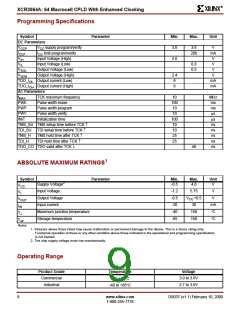
Product Specification
Features
Description
•
•
•
Industry's first TotalCMOS™ PLD - both CMOS design
and process technologies
Fast Zero Power (FZP™) design technique provides
ultra-low power and very high speed
3V, In-System Programmable (ISP) using a JTAG
interface
The XCR3064A CPLD (Complex Programmable Logic
Device) is the second in a family of CoolRunner™ CPLDs
from Xilinx. These devices combine high speed and zero
power in a 64 macrocell CPLD. With the FZP design tech-
nique, the XCR3064A offers true pin-to-pin speeds of 7.5
ns, while simultaneously delivering power that is less than
100 µA at standby without the need for "turbo bits" or other
power down schemes. By replacing conventional sense
amplifier methods for implementing product terms (a tech-
nique that has been used in PLDs since the bipolar era)
with a cascaded chain of pure CMOS gates, the dynamic
power is also substantially lower than any competing
CPLD. These devices are the first TotalCMOS PLDs, as
they use both a CMOS process technology and the pat-
ented full CMOS FZP design technique.
-
-
On-chip superVoltage generation
ISP commands include: Enable, Erase, Program,
Verify
-
-
-
Supported by multiple ISP programming platforms
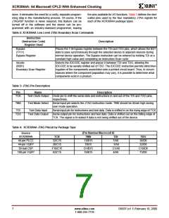
Four pin JTAG interface (TCK, TMS, TDI, TDO)
JTAG commands include: Bypass, Idcode
•
•
•
•
High speed pin-to-pin delays of 7.5 ns
Ultra-low static power of less than 100 µA
5V tolerant I/Os to support mixed Voltage systems
100% routable with 100% utilization while all pins and
all macrocells are fixed
Deterministic timing model that is extremely simple to
use
Up to 12 clocks with programmable polarity at every
macrocell
Support for complex asynchronous clocking
Innovative XPLA™ architecture combines high speed
with extreme flexibility
1000 erase/program cycles guaranteed
20 years data retention guaranteed
Logic expandable to 37 product terms
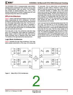
The Xilinx FZP CPLDs utilize the patented XPLA
(eXtended Programmable Logic Array) architecture. The
XPLA architecture combines the best features of both PLA
and PAL type structures to deliver high speed and flexible
logic allocation that results in superior ability to make
design changes with fixed pinouts. The XPLA structure in
each logic block provides a fast 7.5 ns PAL path with five
dedicated product terms per output. This PAL path is joined
by an additional PLA structure that deploys a pool of 32
product terms to a fully programmable OR array that can
allocate the PLA product terms to any output in the logic
block. This combination allows logic to be allocated effi-
ciently throughout the logic block and supports as many as
37 product terms on an output. The speed with which logic
is allocated from the PLA array to an output is only 1.5 ns,
regardless of the number of PLA product terms used, which
•
•
•
•
•
•
•
2
•
•
•
Advanced 0.35µ E CMOS process
Security bit prevents unauthorized access
Design entry and verification using industry standard
and Xilinx CAE tools
•
•
Reprogrammable using industry standard device
programmers
Innovative Control Term structure provides either sum
terms or product terms in each logic block for:
results in worst case t 's of only 9.0 ns from any pin to any
PD
other pin. In addition, logic that is common to multiple out-
puts can be placed on a single PLA product term and
shared across multiple outputs via the OR array, effectively
increasing design density.
-
-
-
Programmable 3-state buffer
Asynchronous macrocell register preset/reset
Up to two asynchronous clocks
The XCR3064A CPLDs are supported by industry standard
CAE tools (Cadence/OrCAD, Exemplar Logic, Mentor, Syn-
opsys, Synario, Viewlogic, and Synplicity), using text
(ABEL, VHDL, Verilog) and/or schematic entry. Design ver-
ification uses industry standard simulators for functional
and timing simulation. Development is supported on per-
sonal computer, Sparc, and HP platforms. Device fitting
uses a Xilinx developed tool, XPLA Professional (available
on the Xilinx web site).
•
•
•
Programmable global 3-state pin facilitates `bed of
nails' testing without using logic resources
Available in PLCC, VQFP, and Chip Scale BGA
packages
Industrial grade operates from 2.7V to 3.6V
DS037 (v1.1) February 10, 2000
www.xilinx.com
1
1-800-255-7778

 XILINX [ XILINX, INC ]