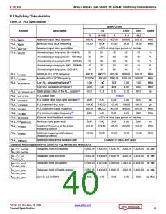
Artix-7 FPGAs Data Sheet: DC and AC Switching Characteristics
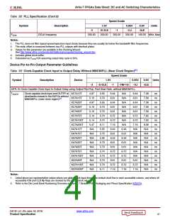
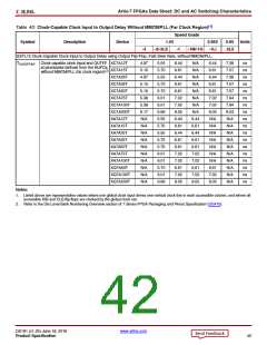
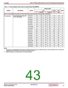
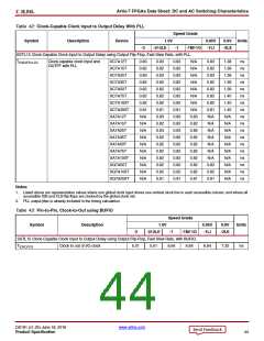
Table 42: Clock-Capable Clock Input to Output Delay With PLL
Speed Grade
Symbol
Description
Device
1.0V
-2/-2LE
SSTL15 Clock-Capable Clock Input to Output Delay using Output Flip-Flop, Fast Slew Rate, with PLL.
0.95V
-1LI
0.9V Units
-2LE
-3
-1
-1M/-1Q
TICKOFPLLCC
Clock-capable clock input and
OUTFF with PLL
XC7A12T
XC7A15T
XC7A25T
XC7A35T
XC7A50T
XC7A75T
XC7A100T
XC7A200T
XA7A12T
XA7A15T
XA7A25T
XA7A35T
XA7A50T
XA7A75T
XA7A100T
XQ7A50T
XQ7A100T
XQ7A200T
0.83
0.82
0.83
0.82
0.82
0.82
0.82
0.81
N/A
N/A
N/A
N/A
N/A
N/A
N/A
N/A
N/A
N/A
0.83
0.82
0.83
0.82
0.82
0.82
0.82
0.81
0.83
0.82
0.83
0.82
0.82
0.82
0.82
0.82
0.82
0.81
0.83
0.82
0.83
0.82
0.82
0.82
0.82
0.81
0.83
0.82
0.83
0.82
0.82
0.82
0.82
0.82
0.82
0.81
N/A
N/A
N/A
N/A
N/A
N/A
N/A
N/A
0.83
0.82
0.83
0.82
0.82
0.82
0.82
0.82
0.82
0.81
0.83
0.82
0.83
0.82
0.82
0.82
0.82
0.81
N/A
N/A
N/A
N/A
N/A
N/A
N/A
1.38
1.39
1.38
1.39
1.39
1.40
1.40
1.45
N/A
N/A
N/A
N/A
N/A
N/A
N/A
N/A
N/A
N/A
ns
ns
ns
ns
ns
ns
ns
ns
ns
ns
ns
ns
ns
ns
ns
ns
ns
ns
0.82
0.82
0.81
Notes:
1. Listed above are representative values where one global clock input drives one vertical clock line in each accessible column, and where all
accessible IOB and CLB flip-flops are clocked by the global clock net.
2. PLL output jitter is already included in the timing calculation.
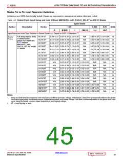
Table 43: Pin-to-Pin, Clock-to-Out using BUFIO
Speed Grade
Symbol
Description
1.0V
-2/-2LE
SSTL15 Clock-Capable Clock Input to Output Delay using Output Flip-Flop, Fast Slew Rate, with BUFIO.
0.95V
-1LI
0.9V
-2LE
Units
-3
-1
-1M/-1Q
TICKOFCS
Clock to out of I/O clock
5.01
5.61
6.64
6.64
6.64
7.32
ns
DS181 (v1.25) June 18, 2018
www.xilinx.com
Product Specification
44

 XILINX [ XILINX, INC ]