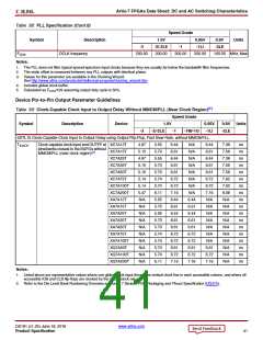
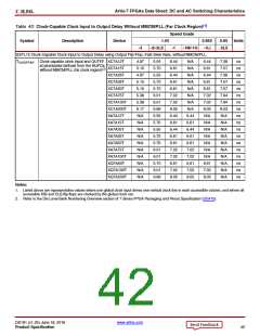
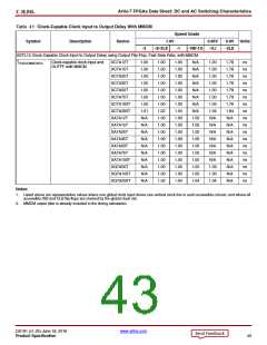
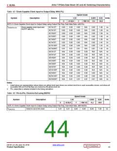
Artix-7 FPGAs Data Sheet: DC and AC Switching Characteristics
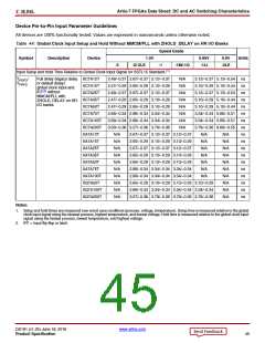
Device Pin-to-Pin Input Parameter Guidelines
All devices are 100% functionally tested. Values are expressed in nanoseconds unless otherwise noted.
Table 44: Global Clock Input Setup and Hold Without MMCM/PLL with ZHOLD_DELAY on HR I/O Banks
Speed Grade
Symbol
Description
Device
1.0V
0.95V
-1LI
0.9V
-2LE
Units
-3
-2/-2LE
-1
-1M/-1Q
Input Setup and Hold Time Relative to Global Clock Input Signal for SSTL15 Standard.(1)
TPSFD
/
Full delay (legacy delay XC7A12T
or default delay)
2.49/–0.37 2.67/–0.37 3.12/–0.37
2.47/–0.29 2.65/–0.29 3.10/–0.29
2.49/–0.37 2.67/–0.37 3.12/–0.37
2.47/–0.29 2.65/–0.29 3.10/–0.29
2.47/–0.29 2.65/–0.29 3.10/–0.29
2.69/–0.34 2.89/–0.34 3.34/–0.34
2.69/–0.34 2.89/–0.34 3.34/–0.34
3.03/–0.36 3.27/–0.36 3.79/–0.36
N/A
N/A
N/A
N/A
N/A
N/A
N/A
N/A
3.12/–0.37 5.13/–0.54
3.10/–0.29 5.10/–0.44
3.12/–0.37 5.13/–0.54
3.10/–0.29 5.10/–0.44
3.10/–0.29 5.10/–0.44
3.34/–0.34 5.66/–0.51
3.34/–0.34 5.66/–0.51
3.79/–0.36 6.66/–0.55
ns
ns
ns
ns
ns
ns
ns
ns
ns
ns
ns
ns
ns
ns
ns
ns
ns
ns
TPHFD
XC7A15T
global clock input and
IFF(2) without
MMCM/PLL with
XC7A25T
XC7A35T
XC7A50T
XC7A75T
XC7A100T
XC7A200T
XA7A12T
XA7A15T
XA7A25T
XA7A35T
XA7A50T
XA7A75T
XA7A100T
XQ7A50T
XQ7A100T
XQ7A200T
ZHOLD_DELAY on HR
I/O banks
N/A
N/A
N/A
N/A
N/A
N/A
N/A
N/A
N/A
N/A
2.67/–0.37 3.12/–0.37 3.12/–0.37
2.65/–0.29 3.10/–0.29 3.10/–0.29
2.67/–0.37 3.12/–0.37 3.12/–0.37
2.65/–0.29 3.10/–0.29 3.10/–0.29
2.65/–0.29 3.10/–0.29 3.10/–0.29
2.89/–0.34 3.34/–0.34 3.34/–0.34
2.89/–0.34 3.34/–0.34 3.34/–0.34
N/A
N/A
N/A
N/A
N/A
N/A
N/A
N/A
N/A
N/A
N/A
N/A
N/A
N/A
N/A
N/A
N/A
2.65/–0.29 3.10/–0.29 3.10/–0.29 3.10/–0.29
2.89/–0.34 3.34/–0.34 3.34/–0.34 3.34/–0.34
3.27/–0.36 3.79/–0.36 3.79/–0.36 3.79/–0.36
Notes:
1. Setup and hold times are measured over worst case conditions (process, voltage, temperature). Setup time is measured relative to the global
clock input signal using the slowest process, highest temperature, and lowest voltage. Hold time is measured relative to the global clock input
signal using the fastest process, lowest temperature, and highest voltage.
2. IFF = Input flip-flop or latch.
DS181 (v1.25) June 18, 2018
www.xilinx.com
Product Specification
45

 XILINX [ XILINX, INC ]