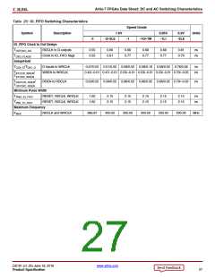
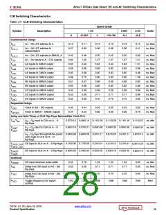
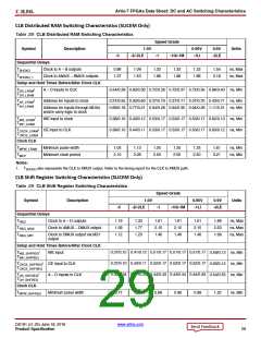
Artix-7 FPGAs Data Sheet: DC and AC Switching Characteristics
Output Serializer/Deserializer Switching Characteristics
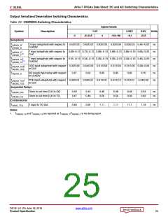
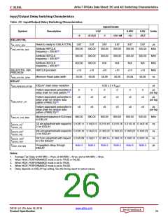
Table 24: OSERDES Switching Characteristics
Speed Grade
Symbol
Description
1.0V
0.95V
-1LI
0.9V
-2LE
Units
-3
-2/-2LE
-1
-1Q/-1M
Setup/Hold
TOSDCK_D
TOSCKD_D
/
D input setup/hold with respect to
CLKDIV
0.42/0.03 0.45/0.03 0.63/0.03 0.63/0.08 0.63/0.03 0.44/–0.02 ns
TOSDCK_T
/
T input setup/hold with respect to 0.69/–0.13 0.73/–0.13 0.88/–0.13 0.88/–0.13 0.88/–0.13 0.66/–0.25 ns
CLK
(1)
TOSCKD_T
TOSDCK_T2
/
T input setup/hold with respect to 0.31/–0.13 0.34/–0.13 0.39/–0.13 0.39/–0.13 0.39/–0.13 0.46/–0.25 ns
CLKDIV
(1)
TOSCKD_T2
TOSCCK_OCE
TOSCKC_OCE
/
OCE input setup/hold with respect 0.32/0.58 0.34/0.58 0.51/0.58 0.51/0.58 0.51/0.58 0.28/–0.04 ns
to CLK
TOSCCK_S
SR (reset) input setup with respect
to CLKDIV
0.47
0.52
0.85
0.85
0.85
0.70
ns
TOSCCK_TCE
/
TCE input setup/hold with respect 0.32/0.01 0.34/0.01 0.51/0.01 0.51/0.10 0.51/0.01 0.24/0.00
to CLK
ns
TOSCKC_TCE
Sequential Delays
TOSCKO_OQ
TOSCKO_TQ
Combinatorial
TOSDO_TTQ
Clock to out from CLK to OQ
0.40
0.47
0.42
0.49
0.48
0.56
0.48
0.56
0.48
0.56
0.54
0.63
ns
ns
Clock to out from CLK to TQ
T input to TQ Out
0.83
0.92
1.11
1.11
1.11
1.18
ns
Notes:
1.
T
and T
are reported as T
/T
in the timing report.
OSDCK_T2
OSCKD_T2
OSDCK_T OSCKD_T
DS181 (v1.25) June 18, 2018
www.xilinx.com
Product Specification
25

 XILINX [ XILINX, INC ]