Artix-7 FPGAs Data Sheet: DC and AC Switching Characteristics
Input/Output Logic Switching Characteristics
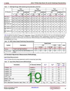
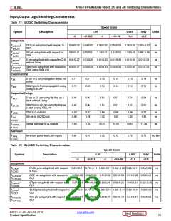
Table 21: ILOGIC Switching Characteristics
Speed Grade
Symbol
Description
1.0V
0.95V
-1LI
0.9V
-2LE
Units
-3
-2/-2LE
-1
-1Q/-1M
Setup/Hold
TICE1CK
TICKCE1
/
CE1 pin setup/hold with respect to
CLK
0.48/0.02 0.54/0.02 0.76/0.02 0.76/0.02 0.76/0.02 0.50/–0.07
0.60/0.01 0.70/0.01 1.13/0.01 1.13/0.01 1.13/0.01 0.88/–0.35
ns
ns
ns
ns
TISRCK
TICKSR
/
SR pin setup/hold with respect to
CLK
TIDOCK
/
D pin setup/hold with respect to CLK 0.01/0.27 0.01/0.29 0.01/0.33 0.01/0.33 0.01/0.33 0.01/0.33
without Delay
TIOCKD
TIDOCKD
TIOCKDD
/
DDLY pin setup/hold with respect to 0.02/0.27 0.02/0.29 0.02/0.33 0.02/0.33 0.02/0.33 0.01/0.33
CLK (using IDELAY)
Combinatorial
TIDI
D pin to O pin propagation delay, no
Delay
0.11
0.11
0.11
0.12
0.13
0.14
0.13
0.14
0.13
0.14
0.14
0.15
ns
ns
TIDID
DDLY pin to O pin propagation delay
(using IDELAY)
Sequential Delays
TIDLO
TIDLOD
TICKQ
D pin to Q1 pin using flip-flop as a
latch without Delay
0.41
0.41
0.44
0.44
0.51
0.51
0.51
0.51
0.51
0.51
0.54
0.55
ns
ns
DDLY pin to Q1 pin using flip-flop as
a latch (using IDELAY)
CLK to Q outputs
0.53
0.96
0.57
1.08
0.66
1.32
0.66
1.32
0.66
1.32
0.71
1.32
ns
ns
TRQ_
SR pin to OQ/TQ out
ILOGIC
TGSRQ_
Global set/reset to Q outputs
7.60
7.60
10.51
10.51
10.51
11.39
ns
ILOGIC
Set/Reset
TRPW_
Minimum pulse width, SR inputs
0.61
0.72
0.72
0.72
0.72
0.72
ns, Min
ILOGIC
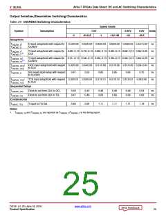
Table 22: OLOGIC Switching Characteristics
Speed Grade
Symbol
Description
1.0V
-2/-2LE
0.95V
-1LI
0.9V
-2LE
Units
-3
-1
-1Q/-1M
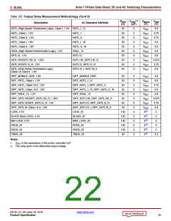
Setup/Hold
TODCK
/
D1/D2 pins setup/hold with respect 0.67/–0.11 0.71/–0.11 0.84/–0.11 0.84/–0.06 0.84/–0.11 0.64/0.03
to CLK
ns
ns
TOCKD
TOOCECK
TOCKOCE
/
OCE pin setup/hold with respect to
CLK
0.32/0.58 0.34/0.58 0.51/0.58 0.51/0.58 0.51/0.58 0.28/0.01
TOSRCK
/
SR pin setup/hold with respect to
CLK
0.37/0.21 0.44/0.21 0.80/0.21 0.80/0.21 0.80/0.21 0.62/–0.25 ns
TOCKSR
TOTCK
TOCKT
/
T1/T2 pins setup/hold with respect to 0.69/–0.14 0.73/–0.14 0.89/–0.14 0.89/–0.11 0.89/–0.14 0.66/0.02
CLK
ns
ns
TOTCECK
TOCKTCE
/
TCE pin setup/hold with respect to
CLK
0.32/0.01 0.34/0.01 0.51/0.01 0.51/0.10 0.51/0.01 0.24/0.05
DS181 (v1.25) June 18, 2018
www.xilinx.com
Product Specification
23

 XILINX [ XILINX, INC ]