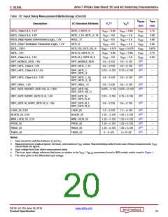
Artix-7 FPGAs Data Sheet: DC and AC Switching Characteristics
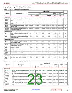
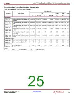
Table 22: OLOGIC Switching Characteristics (Cont’d)
Speed Grade
Symbol
Description
1.0V
0.95V
-1LI
0.9V
-2LE
Units
-3
-2/-2LE
-1
-1Q/-1M
Combinatorial
TODQ
D1 to OQ out or T1 to TQ out
0.83
0.96
1.16
1.16
1.16
1.36
ns
Sequential Delays
TOCKQ
CLK to OQ/TQ out
SR pin to OQ/TQ out
0.47
0.72
7.60
0.49
0.80
7.60
0.56
0.95
0.56
0.95
0.56
0.95
0.63
1.12
ns
ns
ns
TRQ_OLOGIC
TGSRQ_OLOGIC Global set/reset to Q outputs
Set/Reset
10.51
10.51
10.51
11.39
TRPW_OLOGIC Minimum pulse width, SR inputs
0.64
0.74
0.74
0.74
0.74
0.74
ns,
Min
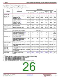
Input Serializer/Deserializer Switching Characteristics
Table 23: ISERDES Switching Characteristics
Speed Grade
Symbol
Description
1.0V
0.95V
-1LI
0.9V
-2LE
Units
-3
-2/-2LE
-1
-1Q/-1M
Setup/Hold for Control Lines
TISCCK_BITSLIP
/
BITSLIP pin setup/hold with
respect to CLKDIV
0.01/0.14 0.02/0.15 0.02/0.17 0.02/0.17 0.02/0.17 0.02/0.21
ns
ns
ns
TISCKC_BITSLIP
TISCCK_CE
TISCKC_CE
/
CE pin setup/hold with respect to 0.45/–0.01 0.50/–0.01 0.72/–0.01 0.72/–0.01 0.72/–0.01 0.45/–0.11
CLK (for CE1)
(2)
TISCCK_CE2
/
CE pin setup/hold with respect to –0.10/0.33 –0.10/0.36 –0.10/0.40 –0.10/0.40 –0.10/0.40 –0.17/0.40
CLKDIV (for CE2)
(2)
TISCKC_CE2
Setup/Hold for Data Lines
TISDCK_D
/
D pin setup/hold with respect to –0.02/0.12 –0.02/0.14 –0.02/0.17 –0.02/0.17 –0.02/0.17 –0.04/0.19
CLK
ns
ns
ns
ns
TISCKD_D
TISDCK_DDLY
TISCKD_DDLY
/
DDLYpin setup/holdwith respect –0.02/0.12 –0.02/0.14 –0.02/0.17 –0.02/0.17 –0.02/0.17 –0.03/0.19
to CLK (using IDELAY)(1)
TISDCK_D_DDR
TISCKD_D_DDR
/
D pin setup/hold with respect to –0.02/0.12 –0.02/0.14 –0.02/0.17 –0.02/0.17 –0.02/0.17 –0.04/0.19
CLK at DDR mode
TISDCK_DDLY_DDR
TISCKD_DDLY_DDR CLK at DDR mode (using
/
D pin setup/hold with respect to 0.12/0.12 0.14/0.14 0.17/0.17 0.17/0.17 0.17/0.17 0.19/0.19
IDELAY)(1)
Sequential Delays
TISCKO_Q
CLKDIV to out at Q pin
D input to DO output pin
0.53
0.11
0.54
0.11
0.66
0.13
0.66
0.13
0.66
0.13
0.67
0.14
ns
ns
Propagation Delays
TISDO_DO
Notes:
1. Recorded at 0 tap value.
2. and T
T
are reported as T
/T
in the timing report.
ISCCK_CE2
ISCKC_CE2
ISCCK_CE ISCKC_CE
DS181 (v1.25) June 18, 2018
www.xilinx.com
Product Specification
24

 XILINX [ XILINX, INC ]