Artix-7 FPGAs Data Sheet: DC and AC Switching Characteristics
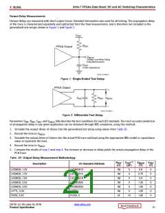
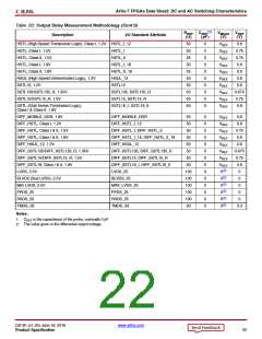
Output Delay Measurements
Output delays are measured with short output traces. Standard termination was used for all testing. The propagation delay
of the trace is characterized separately and subtracted from the final measurement, and is therefore not included in the
generalized test setups shown in Figure 1 and Figure 2.
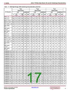
X-Ref Target - Figure 1
VREF
RREF
FPGA Output
VMEAS
(Voltage Level When Taking
Delay Measurement)
CREF
(Probe Capacitance)
DS181_04_090514
Figure 1: Single-Ended Test Setup
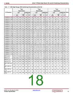
X-Ref Target - Figure 2
FPGA Output
+
CREF
RREF VMEAS
–
DS181_05_090514
Figure 2: Differential Test Setup
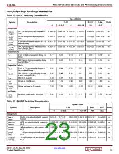
Parameters V , R , C , and V
fully describe the test conditions for each I/O standard. The most accurate prediction
MEAS
REF REF REF
of propagation delay in any given application can be obtained through IBIS simulation, using this method:
1. Simulate the output driver of choice into the generalized test setup using values from Table 20.
2. Record the time to V
.
MEAS
3. Simulate the output driver of choice into the actual PCB trace and load using the appropriate IBIS model or capacitance
value to represent the load.
4. Record the time to V
.
MEAS
5. Compare the results of step 2 and step 4. The increase or decrease in delay yields the actual propagation delay of the
PCB trace.
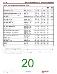
Table 20: Output Delay Measurement Methodology
(1)
RREF CREF
VMEAS VREF
Description
I/O Standard Attribute
LVCMOS12
(Ω)
1M
1M
1M
1M
1M
1M
25
(pF)
0
(V)
(V)
LVCMOS, 1.2V
LVCMOS, 1.5V
LVCMOS, 1.8V
LVCMOS, 2.5V
LVCMOS, 3.3V
LVTTL, 3.3V
0.6
0
LVCMOS15
LVCMOS18
LVCMOS25
LVCMOS33
LVTTL
0
0.75
0.9
0
0
0
0
1.25
1.65
1.65
1.65
0
0
0
0
0
PCI33, 3.3V
PCI33_3
10
0
DS181 (v1.25) June 18, 2018
www.xilinx.com
Product Specification
21

 XILINX [ XILINX, INC ]