Virtex-6 FPGA Data Sheet: DC and Switching Characteristics
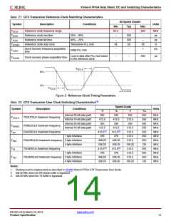
Table 21: GTX Transceiver Reference Clock Switching Characteristics
All Speed Grades
Symbol
Description
Conditions
Units
Min
62.5
–
Typ
–
Max
650
–
FGCLK
TRCLK
TFCLK
TDCREF
Reference clock frequency range
Reference clock rise time
Reference clock fall time
MHz
ps
20% – 80%
200
200
50
–
80% – 20%
–
–
ps
Reference clock duty cycle
Transceiver PLL only
45
–
55
1
%
Clock recovery frequency acquisition
time
ms
TLOCK
Initial PLL lock
Lock to data after PLL has locked
to the reference clock
–
–
200
µs
TPHASE
Clock recovery phase acquisition time
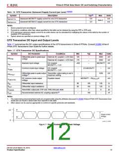
X-Ref Target - Figure 3
TRCLK
80%
20%
TFCLK
ds152_05_042109
Figure 3: Reference Clock Timing Parameters
(1)
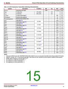
Table 22: GTX Transceiver User Clock Switching Characteristics
Speed Grade
Symbol
Description
Conditions
Units
-3
-2
-1
-1L
250
250
250
250
250
250
250
125
250
250
250
125
Internal 20-bit data path
Internal 16-bit data path
Internal 20-bit data path
Internal 16-bit data path
330
330
250
MHz
MHz
MHz
MHz
MHz
MHz
MHz
MHz
MHz
MHz
MHz
MHz
FTXOUT
TXOUTCLK maximum frequency
412.5
330
412.5
330
312.5
250
FRXREC
TRX
RXRECCLK maximum frequency
RXUSRCLK maximum frequency
412.5
412.5(2)
376
412.5
412.5(2)
376
312.5
312.5
312.5
312.5
156.25
312.5
312.5
312.5
156.25
1 byte interface
TRX2
RXUSRCLK2 maximum frequency 2 byte interface
4 byte interface
406.25
206.25
412.5(3)
376
406.25
206.25
412.5(3)
376
TTX
TXUSRCLK maximum frequency
1 byte interface
TTX2
TXUSRCLK2 maximum frequency 2 byte interface
4 byte interface
406.25
206.25
406.25
206.25
Notes:
1. Clocking must be implemented as described in UG366:Virtex-6 FPGA GTX Transceivers User Guide.
2. 406.25 MHz when the RX elastic buffer is bypassed.
3. 406.25 MHz when the TX buffer is bypassed.
DS152 (v3.6) March 18, 2014
www.xilinx.com
Product Specification
14

 XILINX [ XILINX, INC ]