Virtex-6 FPGA Data Sheet: DC and Switching Characteristics
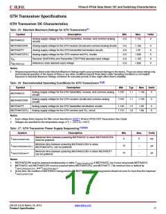
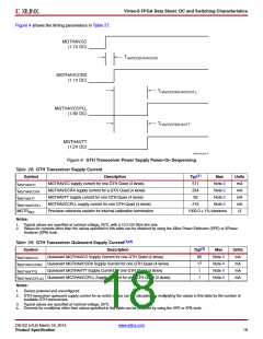
Figure 4 shows the timing parameters in Table 27.
X-Ref Target - Figure 4
MGTHAVCC
(1.1V DC)
THAVCC2HAVCCRX
MGTHAVCCRX
(1.1V DC)
THAVCCRX2HAVCCPLL
MGTHAVCCPLL
(1.8V DC)
THAVCCRX2HAVTT
MGTHAVTT
(1.2V DC)
DS152_04_051110
Figure 4: GTH Transceiver Power Supply Power-On Sequencing
Table 28: GTH Transceiver Supply Current
(1)
Symbol
Description
Typ
Max
Units
mA
mA
mA
mA
Ω
IMGTHAVCC
IMGTHAVCCRX
IMGTHAVTT
MGTHAVCC supply current for one GTH Quad (4 lanes)
MGTHAVCCRX supply current for a GTH Quad (4 lanes)
MGTHAVTT supply current for one GTH Quad (4 lanes)
MGTHAVCCPLL supply current for one GTH Quad (4 lanes)
Precision reference resistor for internal calibration termination
571
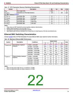
Note 2
Note 2
Note 2
Note 2
254
93
IMGTHAVCCPLL
MGTRREF
219
1000.0 1% tolerance
Notes:
1. Typical values are specified at nominal voltage, 25°C, with a 10.3125 Gb/s line rate.
2. Values for currents other than the values specified in this table can be obtained by using the Xilinx Power Estimator (XPE) or XPower
Analyzer (XPA) tools.
(1)(2)
Table 29: GTH Transceiver Quiescent Supply Current
(3)
Symbol
Description
Typ
65
17
1
Max
Units
mA
IMGTHAVCCQ
Quiescent MGTHAVCC Supply Current for one GTH Quad (4 lanes)
Note 4
Note 4
Note 4
Note 4
IMGTHAVCCRXQ Quiescent MGTHAVCCRX Supply Current for one GTH Quad (4 lanes)
IMGTHAVTTQ Quiescent MGTHAVTT Supply Current for one GTH Quad (4 lanes)
mA
mA
IMGTHAVCCPLLQ Quiescent MGTHAVCCPLL Supply Current for one GTH Quad (4 lanes)
1
mA
Notes:
1. Device powered and unconfigured.
2. GTH transceiver quiescent supply current for an entire device can be calculated by multiplying the values in this table by the number of
available GTH transceivers.
3. Typical values are specified at nominal voltage, 25°C.
4. Currents for conditions other than values specified in this table can be obtained by using the XPE or XPA tools.
DS152 (v3.6) March 18, 2014
www.xilinx.com
Product Specification
18

 XILINX [ XILINX, INC ]