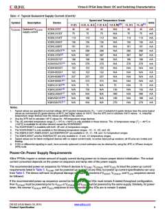
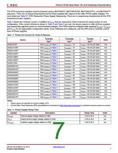
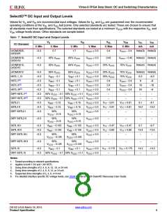
Virtex-6 FPGA Data Sheet: DC and Switching Characteristics
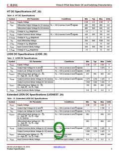
LVPECL DC Specifications (LVPECL_25)
These values are valid when driving a 100Ω differential load only, i.e., a 100Ω resistor between the two receiver pins. The
levels are 200 mV below standard LVPECL levels and are compatible with devices tolerant of lower common-mode
V
OH
ranges. Table 11 summarizes the DC output specifications of LVPECL. For more information on using LVPECL, see UG361:
Virtex-6 FPGA SelectIO Resources User Guide.
Table 11: LVPECL DC Specifications
Symbol
VOH
DC Parameter
Output High Voltage
Min
VCC – 1.025
VCC – 1.81
0.6
Typ
1.545
0.795
–
Max
VCC – 0.88
VCC – 1.62
2.2
Units
V
V
V
V
VOL
Output Low Voltage
VICM
VIDIFF
Input Common-Mode Voltage
Differential Input Voltage(1)(2)
0.100
–
1.5
Notes:
1. Recommended input maximum voltage not to exceed V
+ 0.2V.
CCAUX
2. Recommended input minimum voltage not to go below –0.5V.
eFUSE Read Endurance
Table 12 lists the maximum number of read cycle operations expected. For more information, see UG360:Virtex-6 FPGA
Configuration User Guide.
Table 12: eFUSE Read Endurance
Speed Grade
Symbol
Description
Units
-3
-2
-1
-1L
DNA_CYCLES
Number of DNA_PORT READ operations or JTAG ISC_DNA read
command operations. Unaffected by SHIFT operations.
Read
Cycles
30,000,000
30,000,000
AES_CYCLES
Number of JTAG FUSE_KEY or FUSE_CNTL read command
operations. Unaffected by SHIFT operations.
Read
Cycles
DS152 (v3.6) March 18, 2014
www.xilinx.com
Product Specification
10

 XILINX [ XILINX, INC ]