Virtex-6 FPGA Data Sheet: DC and Switching Characteristics
(1)(2)(3)
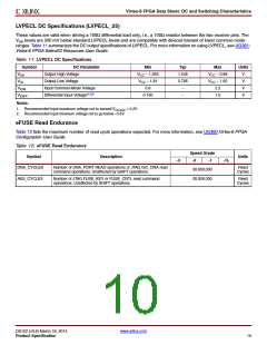
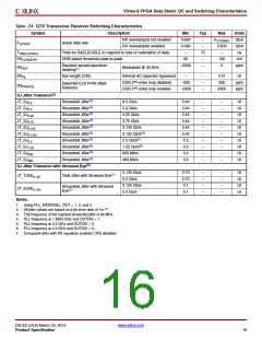
Table 16: GTX Transceiver Quiescent Supply Current (per Lane)
Symbol
IMGTAVTTQ
IMGTAVCCQ
Description
Typ(4)
0.9
Max
Units
mA
Quiescent MGTAVTT supply current for one GTX transceiver
Quiescent MGTAVCC supply current for one GTX transceiver
Note 2
3.5
mA
Notes:
1. Device powered and unconfigured.
2. Currents for conditions other than values specified in this table can be obtained by using the XPE or XPA tools.
3. GTX transceiver quiescent supply current for an entire device can be calculated by multiplying the values in this table by the number of
available GTX transceivers.
4. Typical values are specified at nominal voltage, 25°C.
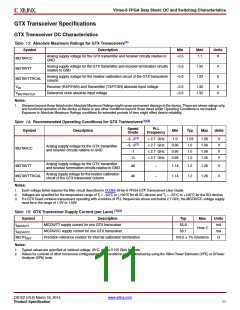
GTX Transceiver DC Input and Output Levels
Table 17 summarizes the DC output specifications of the GTX transceivers in Virtex-6 FPGAs. Consult UG366:Virtex-6
FPGA GTX Transceivers User Guide for further details.
Table 17: GTX Transceiver DC Specifications
Symbol
DC Parameter
Conditions
Min
125
Typ
–
Max
2000
Units
mV
Differential peak-to-peak input External AC coupled ≤ 4.25 Gb/s
DVPPIN
voltage
External AC coupled > 4.25 Gb/s
175
–
2000
mV
Absolute input voltage
DC coupled
MGTAVTT = 1.2V
–400
–
MGTAVTT
mV
VIN
Common mode input voltage
DC coupled
MGTAVTT = 1.2V
–
–
2/3 MGTAVTT
–
–
mV
mV
mV
VCMIN
Differential peak-to-peak output Transmitter output swing is set to
1000
DVPPOUT
VCMOUTDC
voltage(1)
maximum setting
DC common mode output
voltage.
Equation based
MGTAVTT – DVPPOUT/4
RIN
Differential input resistance
Differential output resistance
80
80
–
100
100
2
130
120
8
Ω
Ω
ROUT
TOSKEW
CEXT
Transmitter output pair (TXP and TXN) intra-pair skew
Recommended external AC coupling capacitor(2)
ps
nF
–
100
–
Notes:
1. The output swing and preemphasis levels are programmable using the attributes discussed in UG366:Virtex-6 FPGA GTX Transceivers User
Guide and can result in values lower than reported in this table.
2. Other values can be used as appropriate to conform to specific protocols and standards.
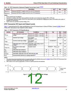
X-Ref Target - Figure 1
+V
0
P
N
Single-Ended
Voltage
ds152_01_121509
Figure 1: Single-Ended Peak-to-Peak Voltage
DS152 (v3.6) March 18, 2014
www.xilinx.com
Product Specification
12

 XILINX [ XILINX, INC ]