Virtex-6 FPGA Data Sheet: DC and Switching Characteristics
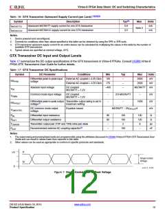
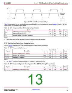
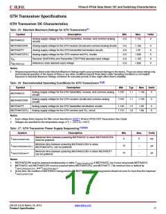
X-Ref Target - Figure 2
+V
0
Differential
Voltage
P–N
–V
ds152_02_121509
Figure 2: Differential Peak-to-Peak Voltage
Table 18 summarizes the DC specifications of the clock input of the GTX transceiver. Consult UG366:Virtex-6 FPGA GTX
Transceivers User Guide for further details.
Table 18: GTX Transceiver Clock DC Input Level Specification
Symbol
VIDIFF
DC Parameter
Differential peak-to-peak input voltage
Min
210
90
Typ
800
100
100
Max
2000
130
–
Units
mV
Ω
RIN
Differential input resistance
CEXT
Required external AC coupling capacitor(1)
–
nF
Notes:
1. Other values can be used as appropriate to conform to specific protocols and standards.
GTX Transceiver Switching Characteristics
Consult UG366:Virtex-6 FPGA GTX Transceivers User Guide for further information.
Table 19: GTX Transceiver Performance
Speed Grade
Symbol
Description
Units
-3
6.6
-2
6.6
-1
-1L
5.0
2.7
1.2
FGTXMAX
FGPLLMAX
FGPLLMIN
Maximum GTX transceiver data rate
Maximum PLL frequency
5.0
2.7
1.2
Gb/s
GHz
GHz
3.3(1)
1.2
3.3(1)
1.2
Minimum PLL frequency
Notes:
1. See Table 14 for MGTAVCC requirements when PLL frequency is greater than 2.7 GHz.
Table 20: GTX Transceiver Dynamic Reconfiguration Port (DRP) Switching Characteristics
Speed Grade
Symbol
Description
Units
-3
-2
-1
-1L
FGTXDRPCLK
GTXDRPCLK maximum frequency
150
150
125
100
MHz
DS152 (v3.6) March 18, 2014
www.xilinx.com
Product Specification
13

 XILINX [ XILINX, INC ]