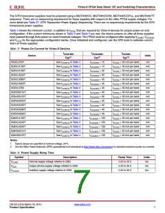
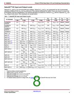
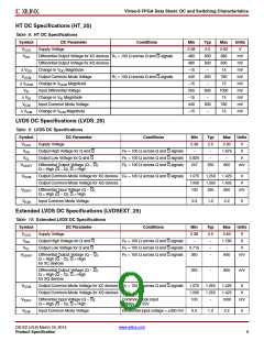
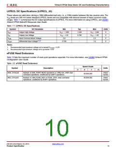
Virtex-6 FPGA Data Sheet: DC and Switching Characteristics
GTX Transceiver Specifications
GTX Transceiver DC Characteristics
(1)
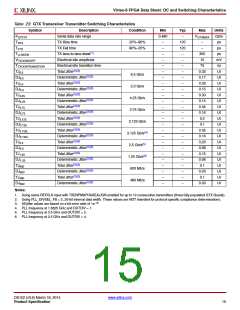
Table 13: Absolute Maximum Ratings for GTX Transceivers
Symbol
Description
Min
Max
Units
Analog supply voltage for the GTX transmitter and receiver circuits relative to
GND
–0.5
1.1
V
MGTAVCC
Analog supply voltage for the GTX transmitter and receiver termination circuits
relative to GND
–0.5
–0.5
1.32
1.32
V
V
MGTAVTT
Analog supply voltage for the resistor calibration circuit of the GTX transceiver
column
MGTAVTTRCAL
VIN
Receiver (RXP/RXN) and Transmitter (TXP/TXN) absolute input voltage
Reference clock absolute input voltage
–0.5
–0.5
1.32
1.32
V
V
VMGTREFCLK
Notes:
1. Stresses beyond those listed under Absolute Maximum Ratings might cause permanent damage to the device. These are stress ratings only,
and functional operation of the device at these or any other conditions beyond those listed under Operating Conditions is not implied.
Exposure to Absolute Maximum Ratings conditions for extended periods of time might affect device reliability.
(1)(2)
Table 14: Recommended Operating Conditions for GTX Transceivers
Speed
Grade
PLL
Frequency
Symbol
Description
Min
Typ
Max
Units
-3, -2(3)
-3, -2(3)
-1
> 2.7 GHz
≤ 2.7 GHz
≤ 2.7 GHz
≤ 2.7 GHz
1.0
1.03
1.0
1.06
1.06
1.06
1.05
V
V
V
V
0.95
0.95
0.95
Analog supply voltage for the GTX transmitter
and receiver circuits relative to GND
MGTAVCC
1.0
-1L
1.0
Analog supply voltage for the GTX transmitter
and receiver termination circuits relative to GND
MGTAVTT
All
All
–
–
1.14
1.14
1.2
1.2
1.26
1.26
V
V
Analog supply voltage for the resistor calibration
circuit of the GTX transceiver column
MGTAVTTRCAL
Notes:
1. Each voltage listed requires the filter circuit described in UG366:Virtex-6 FPGA GTX Transceivers User Guide.
2. Voltages are specified for the temperature range of T = –40°C to +100°C for all XC devices and T = –55°C to +125°C for the XQ devices
j
j
3. If a GTX Quad contains transceivers operating with a mixture of PLL frequencies above and below 2.7 GHz, the MGTAVCC voltage supply
must be in the range of 1.0V to 1.06V.
(1)(2)
Table 15: GTX Transceiver Supply Current (per Lane)
Symbol
IMGTAVTT
Description
Typ
55.9
56.1
Max
Units
mA
mA
Ω
MGTAVTT supply current for one GTX transceiver
MGTAVCC supply current for one GTX transceiver
Precision reference resistor for internal calibration termination
Note 2
IMGTAVCC
MGTRREF
100.0 1% tolerance
Notes:
1. Typical values are specified at nominal voltage, 25°C, with a 3.125 Gb/s line rate.
2. Values for currents of other transceiver configurations and conditions can be obtained by using the Xilinx Power Estimator (XPE) or XPower
Analyzer (XPA) tools.
DS152 (v3.6) March 18, 2014
www.xilinx.com
Product Specification
11

 XILINX [ XILINX, INC ]