Virtex-6 FPGA Data Sheet: DC and Switching Characteristics
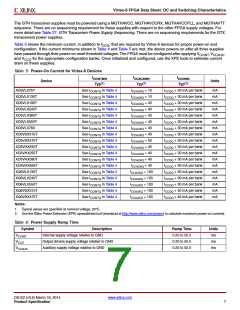
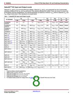
SelectIO™ DC Input and Output Levels
Values for V and V are recommended input voltages. Values for I and I are guaranteed over the recommended
IL
IH
OL
OH
operating conditions at the V and V test points. Only selected standards are tested. These are chosen to ensure that
OL
OH
all standards meet their specifications. The selected standards are tested at a minimum V
with the respective V and
CCO
OL
V
voltage levels shown. Other standards are sample tested.
OH
Table 7: SelectIO DC Input and Output Levels
VIL
VIH
VOL
V, Max
0.4
VOH
IOL
IOH
mA
I/O Standard
V, Min
V, Max
V, Min
V, Max
V, Min
mA
LVCMOS25,
LVDCI25
–0.3
0.7
1.7
VCCO + 0.3
VCCO – 0.4
Note(3) Note(3)
Note(4) Note(4)
Note(4) Note(4)
Note(5) Note(5)
LVCMOS18,
LVDCI18
–0.3
–0.3
35% VCCO
35% VCCO
35% VCCO
65% VCCO
65% VCCO
VCCO + 0.3
VCCO + 0.3
0.45
VCCO – 0.45
75% VCCO
LVCMOS15,
LVDCI15
25% VCCO
LVCMOS12
HSTL I_12
HSTL I(2)
–0.3
–0.3
–0.3
–0.3
–0.3
–0.3
–0.3
–0.3
–0.3
–0.3
65% VCCO
VREF + 0.1
VREF + 0.1
VREF + 0.1
VREF + 0.1
VCCO + 0.3
VCCO + 0.3
VCCO + 0.3
VCCO + 0.3
VCCO + 0.3
25% VCCO
75% VCCO
75% VCCO
VCCO – 0.4
VCCO – 0.4
VCCO – 0.4
–
V
REF – 0.1
25% VCCO
6.3
8
–6.3
–8
VREF – 0.1
VREF – 0.1
VREF – 0.1
0.4
HSTL II(2)
0.4
16
24
–
–16
–8
HSTL III(2)
DIFF HSTL I(2)
DIFF HSTL II(2)
SSTL2 I
0.4
50% VCCO – 0.1 50% VCCO + 0.1 VCCO + 0.3
50% VCCO – 0.1 50% VCCO + 0.1 VCCO + 0.3
–
–
–
–
–
–
VREF – 0.15
VREF + 0.15
VREF + 0.15
VCCO + 0.3
VCCO + 0.3
VTT – 0.61
VTT – 0.81
–
VTT + 0.61
VTT + 0.81
–
8.1
16.2
–
–8.1
–16.2
–
SSTL2 II
VREF – 0.15
DIFF SSTL2 I
50%
50%
VCCO + 0.3
VCCO – 0.15
VCCO + 0.15
DIFF SSTL2 II
–0.3
50%
VCCO – 0.15
50%
VCCO + 0.15
VCCO + 0.3
–
–
–
–
SSTL18 I
–0.3
–0.3
–0.3
VREF – 0.125
VREF – 0.125
VREF + 0.125
VREF + 0.125
VCCO + 0.3
VCCO + 0.3
VTT – 0.47
VTT – 0.60
–
VTT + 0.47
VTT + 0.60
–
6.7
13.4
–
–6.7
–13.4
–
SSTL18 II
DIFF SSTL18 I
50%
VCCO – 0.125
50%
VCCO + 0.125
VCCO + 0.3
DIFF SSTL18 II
–0.3
50%
VCCO – 0.125
50%
VCCO + 0.125
VCCO + 0.3
VCCO + 0.3
–
–
–
–
SSTL15
–0.3
–0.3
VREF – 0.1
VREF + 0.1
VTT – 0.175
–
VTT + 0.175
–
14.3
–
–14.3
–
DIFF SSTL15
50% VCCO – 0.1 50% VCCO + 0.1 VCCO + 0.3
Notes:
1. Tested according to relevant specifications.
2. Applies to both 1.5V and 1.8V HSTL.
3. Using drive strengths of 2, 4, 6, 8, 12, 16, or 24 mA.
4. Using drive strengths of 2, 4, 6, 8, 12, or 16 mA.
5. Supported drive strengths of 2, 4, 6, or 8 mA.
6. For detailed interface specific DC voltage levels, see UG361:Virtex-6 FPGA SelectIO Resources User Guide.
DS152 (v3.6) March 18, 2014
www.xilinx.com
Product Specification
8

 XILINX [ XILINX, INC ]