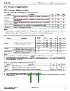
Virtex-6 FPGA Data Sheet: DC and Switching Characteristics
The GTH transceiver supplies must be powered using a MGTHAVCC, MGTHAVCCRX, MGTHAVCCPLL, and MGTHAVTT
sequence. There are no sequencing requirement for these supplies with respect to the other FPGA supply voltages. For
more detail see Table 27: GTH Transceiver Power Supply Sequencing. There are no sequencing requirements for the GTX
transceivers power supplies.
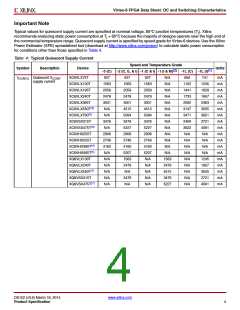
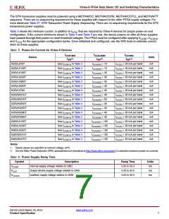
Table 5 shows the minimum current, in addition to I
, that are required by Virtex-6 devices for proper power-on and
CCQ
configuration. If the current minimums shown in Table 4 and Table 5 are met, the device powers on after all three supplies
have passed through their power-on reset threshold voltages. The FPGA must be configured after applying V
, V
,
CCINT CCAUX
and V
for the appropriate configuration banks. Once initialized and configured, use the XPE tools to estimate current
CCO
drain on these supplies.
Table 5: Power-On Current for Virtex-6 Devices
ICCINTMIN
ICCAUXMIN
Typ(1)
ICCOMIN
Typ(1)
Device
Units
Typ(1)
XC6VLX75T
See ICCINTQ in Table 4
See ICCINTQ in Table 4
See ICCINTQ in Table 4
See ICCINTQ in Table 4
See ICCINTQ in Table 4
See ICCINTQ in Table 4
See ICCINTQ in Table 4
See ICCINTQ in Table 4
See ICCINTQ in Table 4
See ICCINTQ in Table 4
See ICCINTQ in Table 4
See ICCINTQ in Table 4
See ICCINTQ in Table 4
See ICCINTQ in Table 4
See ICCINTQ in Table 4
See ICCINTQ in Table 4
See ICCINTQ in Table 4
See ICCINTQ in Table 4
ICCAUXQ + 10
ICCAUXQ + 10
ICCAUXQ + 40
ICCAUXQ + 40
ICCAUXQ + 40
ICCAUXQ + 40
ICCAUXQ + 40
ICCAUXQ + 40
ICCAUXQ + 50
ICCAUXQ + 40
ICCAUXQ + 40
ICCAUXQ + 40
ICCAUXQ + 40
ICCAUXQ + 100
ICCAUXQ + 100
ICCAUXQ + 100
ICCAUXQ + 100
ICCAUXQ + 100
ICCOQ + 30 mA per bank
ICCOQ + 30 mA per bank
ICCOQ + 30 mA per bank
ICCOQ + 30 mA per bank
ICCOQ + 30 mA per bank
ICCOQ + 30 mA per bank
ICCOQ + 30 mA per bank
ICCOQ + 30 mA per bank
ICCOQ + 30 mA per bank
ICCOQ + 30 mA per bank
ICCOQ + 30 mA per bank
ICCOQ + 30 mA per bank
ICCOQ + 30 mA per bank
ICCOQ + 30 mA per bank
ICCOQ + 30 mA per bank
ICCOQ + 30 mA per bank
ICCOQ + 40 mA per bank
ICCOQ + 40 mA per bank
mA
mA
mA
mA
mA
mA
mA
mA
mA
mA
mA
mA
mA
mA
mA
mA
mA
mA
XC6VLX130T
XC6VLX195T
XC6VLX240T
XC6VLX365T
XC6VLX550T
XC6VLX760
XC6VSX315T
XC6VSX475T
XC6VHX250T
XC6VHX255T
XC6VHX380T
XC6VHX565T
XQ6VLX130T
XQ6VLX240T
XQ6VLX550T
XQ6VSX315T
XQ6VSX475T
Notes:
1. Typical values are specified at nominal voltage, 25°C.
2. Use the Xilinx Power Estimator (XPE) spreadsheet tool (download at http://www.xilinx.com/power) to calculate maximum power-on currents.
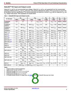
Table 6: Power Supply Ramp Time
Symbol
VCCINT
Description
Internal supply voltage relative to GND
Ramp Time
0.20 to 50.0
0.20 to 50.0
0.20 to 50.0
Units
ms
VCCO
Output drivers supply voltage relative to GND
Auxiliary supply voltage relative to GND
ms
VCCAUX
ms
DS152 (v3.6) March 18, 2014
www.xilinx.com
Product Specification
7

 XILINX [ XILINX, INC ]