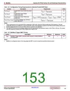
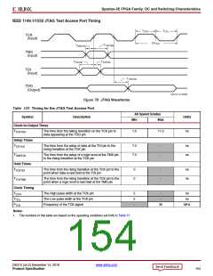
227
Spartan-3E FPGA Family:
Pinout Descriptions
DS312 (v4.2) December 14, 2018
Product Specification
Introduction
Pin Types
This section describes the various pins on a Spartan®-3E
FPGA and how they connect within the supported
component packages.
Most pins on a Spartan-3E FPGA are general-purpose,
user-defined I/O pins. There are, however, up to 11 different
functional types of pins on Spartan-3E packages, as
outlined in Table 124. In the package footprint drawings that
follow, the individual pins are color-coded according to pin
type as in the table.
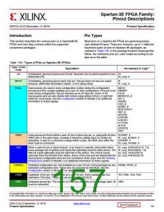
Table 124: Types of Pins on Spartan-3E FPGAs
Type / Color
Description
Code
Pin Name(s) in Type(1)
I/O
Unrestricted, general-purpose user-I/O pin. Most pins can be paired together to form IO
differential I/Os.
IO_Lxxy_#
INPUT
DUAL
Unrestricted, general-purpose input-only pin. This pin does not have an output
structure, differential termination resistor, or PCI clamp diode.
IP
IP_Lxxy_#
Dual-purpose pin used in some configuration modes during the configuration
process and then usually available as a user I/O after configuration. If the pin is not HSWAP
M[2:0]
used during configuration, this pin behaves as an I/O-type pin. Some of the
dual-purpose pins are also shared with bottom-edge global (GCLK) or right-half
(RHCLK) clock inputs. See the Configuration section in Module 2 for additional
information on these signals.
CCLK
MOSI/CSI_B
D[7:1]
D0/DIN
CSO_B
RDWR_B
BUSY/DOUT
INIT_B
A[23:20]
A19/VS2
A18/VS1
A17/VS0
A[16:0]
LDC[2:0]
HDC
VREF
CLK
Dual-purpose pin that is either a user-I/O pin or Input-only pin, or, along with all other IP/VREF_#
VREF pins in the same bank, provides a reference voltage input for certain I/O
standards. If used for a reference voltage within a bank, all VREF pins within the
bank must be connected.
IP_Lxxy_#/VREF_#
IO/VREF_#
IO_Lxxy_#/VREF_#
Either a user-I/O pin or Input-only pin, or an input to a specific clock buffer driver.
IO_Lxxy_#/GCLK[15:10, 7:2]
Every package has 16 global clock inputs that optionally clock the entire device. The IP_Lxxy_#/GCLK[9:8, 1:0]
RHCLK inputs optionally clock the right-half of the device. The LHCLK inputs IO_Lxxy_#/LHCLK[7:0]
optionally clock the left-half of the device. Some of the clock pins are shared with the IO_Lxxy_#/RHCLK[7:0]
dual-purpose configuration pins and are considered DUAL-type. See the Clocking
Infrastructure section in Module 2 for additional information on these signals.
CONFIG
Dedicated configuration pin. Not available as a user-I/O pin. Every package has two DONE, PROG_B
dedicated configuration pins. These pins are powered by VCCAUX. See the
Configuration section in Module 2 for details.
JTAG
GND
Dedicated JTAG pin. Not available as a user-I/O pin. Every package has four
dedicated JTAG pins. These pins are powered by VCCAUX.
TDI, TMS, TCK, TDO
Dedicated ground pin. The number of GND pins depends on the package used. All GND
must be connected.
© Copyright 2005–2018 Xilinx, Inc. XILINX, the Xilinx logo, Virtex, Spartan, ISE, Artix, Kintex, Zynq, Vivado, and other designated brands included herein are trademarks of Xilinx
in the United States and other countries. PCI and PCI-X are trademarks of PCI-SIG and used under license. All other trademarks are the property of their respective owners.
DS312 (v4.2) December 14, 2018
www.xilinx.com
Product Specification
157

 XILINX [ XILINX, INC ]