Spartan-3E FPGA Family: Pinout Descriptions
Mechanical Drawings
Package drawings and package material declaration data
sheets (MDDS) are available on www.xilinx.com.
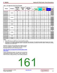
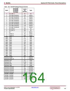
Package Pins by Type
Each package has three separate voltage supply inputs—
VCCINT, VCCAUX, and VCCO—and a common ground
return, GND. The numbers of pins dedicated to these
functions vary by package, as shown in Table 127.
Table 127: Power and Ground Supply Pins by Package
Package
VQ100
CP132
TQ144
PQ208
FT256
VCCINT
VCCAUX
VCCO
8
GND
12
4
6
4
4
8
16
4
4
9
13
4
8
12
16
20
24
28
20
8
8
28
FG320
FG400
FG484
8
8
28
16
16
8
42
10
48
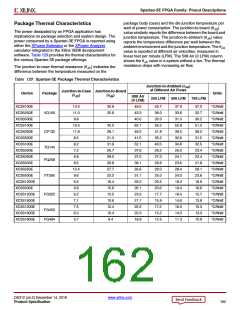
A majority of package pins are user-defined I/O or input
pins. However, the numbers and characteristics of these I/O
depend on the device type and the package in which it is
available, as shown in Table 128. The table shows the
maximum number of single-ended I/O pins available,
assuming that all I/O-, INPUT-, DUAL-, VREF-, and
CLK-type pins are used as general-purpose I/O. Likewise,
the table shows the maximum number of differential
pin-pairs available on the package. Finally, the table shows
how the total maximum user-I/Os are distributed by pin type,
including the number of unconnected—i.e., N.C.—pins on
the device.
DS312 (v4.2) December 14, 2018
www.xilinx.com
Product Specification
160

 XILINX [ XILINX, INC ]