Spartan-3E FPGA Family: Pinout Descriptions
Pin Name(s) in Type(1)
Table 124: Types of Pins on Spartan-3E FPGAs (Cont’d)
Type / Color
Description
Code
VCCAUX
VCCINT
VCCO
Dedicated auxiliary power supply pin. The number of VCCAUX pins depends on the VCCAUX
package used. All must be connected to +2.5V. See the Powering Spartan-3E
FPGAs section in Module 2 for details.
Dedicated internal core logic power supply pin. The number of VCCINT pins
depends on the package used. All must be connected to +1.2V. See the Powering
Spartan-3E FPGAs section in Module 2 for details.
VCCINT
Along with all the other VCCO pins in the same bank, this pin supplies power to the VCCO_#
output buffers within the I/O bank and sets the input threshold voltage for some I/O
standards. See the Powering Spartan-3E FPGAs section in Module 2 for details.
N.C.
This package pin is not connected in this specific device/package combination but N.C.
may be connected in larger devices in the same package.
Notes:
1. # = I/O bank number, an integer between 0 and 3.
2. IRDY/TRDY designations are for PCI designs; refer to PCI documentation for details.
‘L’ indicates that the pin is part of a differential pair.
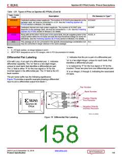
Differential Pair Labeling
‘xx’ is a two-digit integer, unique for each bank, that
identifies a differential pin-pair.
I/Os with Lxxy_# are part of a differential pair. ‘L’ indicates
differential capability. The ‘xx’ field is a two-digit integer,
unique to each bank that identifies a differential pin-pair.
The ‘y’ field is either ‘P’ for the true signal or ‘N’ for the
inverted signal in the differential pair. The ‘#’ field is the I/O
bank number.
‘y’ is replaced by ‘P’ for the true signal or ‘N’ for the
inverted. These two pins form one differential pin-pair.
‘#’ is an integer, 0 through 3, indicating the associated
I/O bank.
The pin name suffix has the following significance.
Figure 79 provides a specific example showing a differential
input to and a differential output from Bank 1.
X-Ref Target - Figure 79
Pair Number
Bank Number
IO_L38P_1
Bank 0
IO_L38N_1
True Receiver
IO_L39P_1
Positive Polarity
Spartan-3E
FPGA
IO_L39N_1
Negative Polarity
Inverted Receiver
Bank 2
DS312-4_00_032409
Figure 79: Differential Pair Labeling
DS312 (v4.2) December 14, 2018
www.xilinx.com
Product Specification
158

 XILINX [ XILINX, INC ]