Spartan-3E FPGA Family: Pinout Descriptions
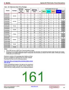
Table 128: Maximum User I/O by Package
Maximum
All Possible I/Os by Type
(2)
Maximum
Input-
Only
Maximum
Differential
Pairs
User I/Os
and
Device
Package
VQ100
I/O
INPUT DUAL VREF(1)
N.C.
CLK
Input-Only
XC3S100E
XC3S250E
XC3S500E
XC3S100E
XC3S250E
XC3S500E
XC3S100E
XC3S250E
XC3S250E
XC3S500E
XC3S250E
XC3S500E
XC3S1200E
XC3S500E
XC3S1200E
XC3S1600E
XC3S1200E
XC3S1600E
XC3S1600E
66
66
7
30
30
30
35
41
41
40
40
65
65
68
77
77
92
99
99
124
124
156
16
16
1
21
21
21
42
46
46
42
42
46
46
46
46
46
46
46
46
46
46
46
4
4
24
24
24
16
16
16
16
16
16
16
16
16
16
16
16
16
16
16
16
0
0
7
1
66
7
16
1
4
0
83
11
7
16
2
7
9
CP132
92
22
0
8
0
92
7
22
0
8
0
108
108
158
158
172
190
190
232
250
250
304
304
376
28
28
32
32
40
41
40
56
56
56
72
72
82
22
19
21
25
25
33
33
31
48
47
47
62
62
72
9
0
TQ144
PQ208
20
9
0
58
13
13
15
19
19
20
21
21
24
24
28
0
58
0
62
18
0
FT256
FG320
76
78
0
102
120
120
156
156
214
18
0
0
0
FG400
FG484
0
0
Notes:
1. Some VREF pins are on INPUT pins. See pinout tables for details.
2. All devices have 24 possible global clock and right- and left-half side clock inputs. The right-half and bottom-edge clock pins have shared
functionality in some FPGA configuration modes. Consequently, some clock pins are counted in the DUAL column. 4 GCLK pins, including
2 DUAL pins, are on INPUT pins.
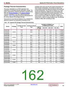
Electronic versions of the package pinout tables and foot-
prints are available for download from the Xilinx website.
Download the files from the following location:
http://www.xilinx.com/support/documentation/data_sheets
/s3e_pin.zip
Using a spreadsheet program, the data can be sorted and
reformatted according to any specific needs. Similarly, the
ASCII-text file is easily parsed by most scripting programs.
DS312 (v4.2) December 14, 2018
www.xilinx.com
Product Specification
161

 XILINX [ XILINX, INC ]