Spartan-3E FPGA Family: DC and Switching Characteristics
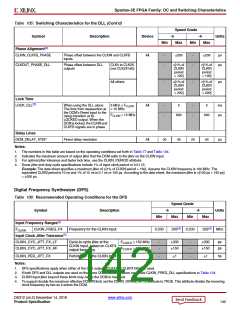
Table 105: Switching Characteristics for the DLL (Cont’d)
Speed Grade
Symbol
Description
Device
-5
-4
Units
Min
Max
Min
Max
Phase Alignment(4)
CLKIN_CLKFB_PHASE
Phase offset between the CLKIN and CLKFB
inputs
All
-
-
200
-
-
200
ps
ps
CLKOUT_PHASE_DLL
Phase offset between DLL
outputs
CLK0 to CLK2X
(not CLK2X180)
[1% of
CLKIN
period
+ 100]
[1% of
CLKIN
period
+ 100]
All others
-
[1% of
CLKIN
period
+ 200]
-
[1% of
CLKIN
period
+ 200]
ps
Lock Time
(3)
LOCK_DLL
When using the DLL alone:
The time from deassertion at ≤ 15 MHz
the DCM’s Reset input to the
5 MHz ≤ F
All
-
-
5
-
-
5
ms
CLKIN
F
> 15 MHz
600
600
μs
CLKIN
rising transition at its
LOCKED output. When the
DCM is locked, the CLKIN and
CLKFB signals are in phase
Delay Lines
DCM_DELAY_STEP
Finest delay resolution
All
20
40
20
40
ps
Notes:
1. The numbers in this table are based on the operating conditions set forth in Table 77 and Table 104.
2. Indicates the maximum amount of output jitter that the DCM adds to the jitter on the CLKIN input.
3. For optimal jitter tolerance and faster lock time, use the CLKIN_PERIOD attribute.
4. Some jitter and duty-cycle specifications include 1% of input clock period or 0.01 UI.
Example: The data sheet specifies a maximum jitter of [1% of CLKIN period + 150]. Assume the CLKIN frequency is 100 MHz. The
equivalent CLKIN period is 10 ns and 1% of 10 ns is 0.1 ns or 100 ps. According to the data sheet, the maximum jitter is [100 ps + 150 ps]
=
250 ps.
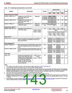
Digital Frequency Synthesizer (DFS)
Table 106: Recommended Operating Conditions for the DFS
Speed Grade
Symbol
Description
-5
-4
Units
Min
Max
Min
Max
Input Frequency Ranges(2)
(4)
(4)
FCLKIN
CLKIN_FREQ_FX
Frequency for the CLKIN input
0.200
333
0.200
333
MHz
Input Clock Jitter Tolerance(3)
CLKIN_CYC_JITT_FX_LF
CLKIN_CYC_JITT_FX_HF
Cycle-to-cycle jitter at the
CLKIN input, based on CLKFX
output frequency
FCLKFX ≤ 150 MHz
FCLKFX > 150 MHz
-
-
300
150
-
-
300
150
ps
ps
CLKIN_PER_JITT_FX
Period jitter at the CLKIN input
-
1
-
1
ns
Notes:
1. DFS specifications apply when either of the DFS outputs (CLKFX or CLKFX180) are used.
2. If both DFS and DLL outputs are used on the same DCM, follow the more restrictive CLKIN_FREQ_DLL specifications in Table 104.
3. CLKIN input jitter beyond these limits may cause the DCM to lose lock.
4. To support double the maximum effective FCLKIN limit, set the CLKIN_DIVIDE_BY_2 attribute to TRUE. This attribute divides the incoming
clock frequency by two as it enters the DCM.
DS312 (v4.2) December 14, 2018
www.xilinx.com
Product Specification
142

 XILINX [ XILINX, INC ]