Spartan-3E FPGA Family: DC and Switching Characteristics
Digital Clock Manager (DCM) Timing
For specification purposes, the DCM consists of three key
components: the Delay-Locked Loop (DLL), the Digital
Frequency Synthesizer (DFS), and the Phase Shifter (PS).
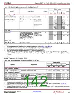
Period jitter is the worst-case deviation from the ideal clock
period over a collection of millions of samples. In a
histogram of period jitter, the mean value is the clock period.
Aspects of DLL operation play a role in all DCM
Cycle-cycle jitter is the worst-case difference in clock period
between adjacent clock cycles in the collection of clock
periods sampled. In a histogram of cycle-cycle jitter, the
mean value is zero.
applications. All such applications inevitably use the CLKIN
and the CLKFB inputs connected to either the CLK0 or the
CLK2X feedback, respectively. Thus, specifications in the
DLL tables (Table 104 and Table 105) apply to any
application that only employs the DLL component. When
the DFS and/or the PS components are used together with
the DLL, then the specifications listed in the DFS and PS
tables (Table 106 through Table 109) supersede any
corresponding ones in the DLL tables. DLL specifications
that do not change with the addition of DFS or PS functions
are presented in Table 104 and Table 105.
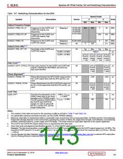
Spread Spectrum
DCMs accept typical spread spectrum clocks as long as
they meet the input requirements. The DLL will track the
frequency changes created by the spread spectrum clock to
drive the global clocks to the FPGA logic. See XAPP469,
Spread-Spectrum Clocking Reception for Displays for
details.
Period jitter and cycle-cycle jitter are two of many different
ways of specifying clock jitter. Both specifications describe
statistical variation from a mean value.
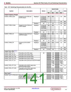
Delay-Locked Loop (DLL)
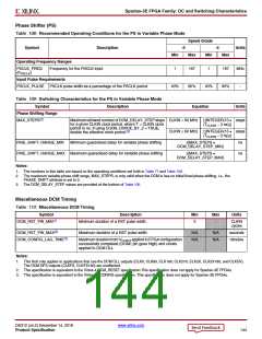
Table 104: Recommended Operating Conditions for the DLL
Speed Grade
Symbol
Description
-5
-4
Units
Min
Max
Min
Max
Input Frequency Ranges
FCLKIN CLKIN_FREQ_DLL Frequency of the CLKIN
clock input
Stepping 0
Stepping 1
XC3S100E
XC3S250E
XC3S500E
XC3S1600E
N/A
N/A
5(2)
90(3)
MHz
XC3S1200E(3)
All
200(3)
240(3)
MHz
MHz
5(2)
275(3)
Input Pulse Requirements
CLKIN_PULSE
CLKIN pulse width as a
percentage of the CLKIN
period
FCLKIN ≤ 150 MHz
40%
45%
60%
55%
40%
45%
60%
55%
-
-
FCLKIN > 150 MHz
Input Clock Jitter Tolerance and Delay Path Variation(4)
CLKIN_CYC_JITT_DLL_LF
CLKIN_CYC_JITT_DLL_HF
CLKIN_PER_JITT_DLL
Cycle-to-cycle jitter at the
CLKIN input
FCLKIN ≤ 150 MHz
FCLKIN > 150 MHz
-
-
-
-
300
150
1
-
-
-
-
300
150
1
ps
ps
ns
ns
Period jitter at the CLKIN input
CLKFB_DELAY_VAR_EXT
Allowable variation of off-chip feedback delay from the DCM
output to the CLKFB input
1
1
Notes:
1. DLL specifications apply when any of the DLL outputs (CLK0, CLK90, CLK180, CLK270, CLK2X, CLK2X180, or CLKDV) are in use.
2. The DFS, when operating independently of the DLL, supports lower FCLKIN frequencies. See Table 106.
3. To support double the maximum effective FCLKIN limit, set the CLKIN_DIVIDE_BY_2 attribute to TRUE. This attribute divides the incoming
clock frequency by two as it enters the DCM. The CLK2X output reproduces the clock frequency provided on the CLKIN input.
4. CLKIN input jitter beyond these limits might cause the DCM to lose lock.
DS312 (v4.2) December 14, 2018
www.xilinx.com
Product Specification
140

 XILINX [ XILINX, INC ]