156
Spartan-3E FPGA Family:
DC and Switching Characteristics
DS312 (v4.2) December 14, 2018
Product Specification
DC Electrical Characteristics
In this section, specifications may be designated as
Advance, Preliminary, or Production. These terms are
defined as follows:
All parameter limits are representative of worst-case supply
voltage and junction temperature conditions. Unless
otherwise noted, the published parameter values apply
to all Spartan®-3E devices. AC and DC characteristics
are specified using the same numbers for both
commercial and industrial grades.
Advance: Initial estimates are based on simulation, early
characterization, and/or extrapolation from the
characteristics of other families. Values are subject to
change. Use as estimates, not for production.
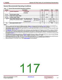
Absolute Maximum Ratings
Preliminary: Based on characterization. Further changes
Stresses beyond those listed under Table 73, Absolute
Maximum Ratings may cause permanent damage to the
device. These are stress ratings only; functional operation
of the device at these or any other conditions beyond those
listed under the Recommended Operating Conditions is not
implied. Exposure to absolute maximum conditions for
extended periods of time adversely affects device reliability.
are not expected.
Production: These specifications are approved once the
silicon has been characterized over numerous production
lots. Parameter values are considered stable with no future
changes expected.
Table 73: Absolute Maximum Ratings
Symbol
VCCINT
VCCAUX
VCCO
Description
Internal supply voltage
Conditions
Min
–0.5
–0.5
–0.5
–0.5
–0.95
–0.85
–0.5
–
Max
1.32
Units
V
Auxiliary supply voltage
Output driver supply voltage
Input reference voltage
3.00
V
3.75
VCCO +0.5(1)
V
VREF
V
(1,2,3,4)
VIN
Voltage applied to all User I/O pins and
Dual-Purpose pins
Driver in a
Commercial
Industrial
4.4
V
high-impedance
state
4.3
V
Voltage applied to all Dedicated pins
Input clamp current per I/O pin
Electrostatic Discharge Voltage
All temp. ranges
V
CCAUX+0.5(3)
V
IIK
–0.5 V < VIN < (VCCO + 0.5 V)
Human body model
100
mA
V
VESD
–
2000
500
Charged device model
Machine model
–
V
–
200
V
TJ
Junction temperature
Storage temperature
–
125
°C
°C
TSTG
–65
150
Notes:
1. Each of the User I/O and Dual-Purpose pins is associated with one of the four banks’ V
rails. Keeping V within 500 mV of the
CCO
IN
associated V
rails or ground rail ensures that the internal diode junctions do not turn on. Table 77 specifies the V
range used to
CCO
CCO
evaluate the maximum V voltage.
IN
2. Input voltages outside the -0.5V to V
+ 0.5V (or V
+ 0.5V) voltage range are require the I input diode clamp diode rating is met
CCAUX IK
CCO
and no more than 100 pins exceed the range simultaneously. Prolonged exposure to such current may compromise device reliability. A
sustained current of 10 mA will not compromise device reliability. See XAPP459: Eliminating I/O Coupling Effects when Interfacing
Large-Swing Single-Ended Signals to User I/O Pins on Spartan-3 Families for more details.
3. All Dedicated pins (PROG_B, DONE, TCK, TDI, TDO, and TMS) draw power from the V
rail (2.5V). Meeting the V max limit ensures
CCAUX
IN
that the internal diode junctions that exist between each of these pins and the V
rail do not turn on. Table 77 specifies the V
CCAUX
CCAUX
range used to evaluate the maximum V voltage. As long as the V max specification is met, oxide stress is not possible.
IN
IN
4. See XAPP459: Eliminating I/O Coupling Effects when Interfacing Large-Swing Single-Ended Signals to User I/O Pins on Spartan-3
Families.
5. For soldering guidelines, see UG112: Device Packaging and Thermal Characteristics and XAPP427: Implementation and Solder Reflow
Guidelines for Pb-Free Packages.
© Copyright 2005–2018 Xilinx, Inc. XILINX, the Xilinx logo, Virtex, Spartan, ISE, Artix, Kintex, Zynq, Vivado, and other designated brands included herein are trademarks of Xilinx
in the United States and other countries. PCI and PCI-X are trademarks of PCI-SIG and used under license. All other trademarks are the property of their respective owners.
DS312 (v4.2) December 14, 2018
www.xilinx.com
Product Specification
115

 XILINX [ XILINX, INC ]