Spartan-3E FPGA Family: Functional Description
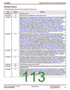
Revision History
The following table shows the revision history for this document.
Date
Version
1.0
Revision
03/01/2005
03/21/2005
11/23/2005
Initial Xilinx release.
1.1
Updated Figure 45. Modified title on Table 39 and Table 45.
2.0
Updated values of On-Chip Differential Termination resistors. Updated Table 7. Updated configuration
bitstream sizes for XC3S250E through XC3S1600E in Table 45, Table 51, Table 57, and Table 60.
Added DLL Performance Differences Between Steppings. Added Stepping 0 Limitations when
Reprogramming via JTAG if FPGA Set for BPI Configuration. Added Stepping 0 limitations when
Daisy-Chaining in SPI configuration mode. Added Multiplier/Block RAM Interaction section. Updated
Digital Clock Managers (DCMs) section, especially Phase Shifter (PS) portion. Corrected and
enhanced the clock infrastructure diagram in Figure 45 and Table 41. Added CCLK Design
Considerations section. Added Design Considerations for the HSWAP, M[2:0], and VS[2:0] Pins
section. Added Spansion, Winbond, and Macronix to list of SPI Flash vendors in Table 53 and Table 56.
Clarified that SPI mode configuration supports Atmel ‘C’- and ‘D’-series DataFlash. Updated the
Programming Support section for SPI Flash PROMs. Added Power-On Precautions if PROM Supply is
Last in Sequence, Compatible Flash Families, and BPI Mode Interaction with Right and Bottom Edge
Global Clock Inputs sections to BPI configuration mode topic. Updated and amplified Powering
Spartan-3E FPGAs section. Added Production Stepping section.
03/22/2006
3.0
Upgraded data sheet status to Preliminary. Updated Input Delay Functions and Figure 6. Added
clarification that Input-only pins also have Pull-Up and Pull-Down Resistors. Added design note about
address setup and hold requirements to Block RAM. Added warning message about software
differences between ISE 8.1i, Service Pack 3 and earlier software to FIXED Phase Shift Mode and
VARIABLE Phase Shift Mode. Added message about using GCLK1 in DLL Clock Input Connections
and Clock Inputs. Updated Figure 45. Added additional information on HSWAP behavior to Pin
Behavior During Configuration. Highlighted which pins have configuration pull-up resistors unaffected
by HSWAP in Table 46. Updated bitstream image sizes for the XC3S1200E and XC3S1600E in
Table 45, Table 51, Table 57, and Table 60. Clarified that ‘B’-series Atmel DataFlash SPI PROMs can
be used in Commercial temperature range applications in Table 53 and Figure 54. Updated Figure 56.
Updated Dynamically Loading Multiple Configuration Images Using MultiBoot Option section. Added
design note about BPI daisy-chaining software support to BPI Daisy-Chaining section. Updated JTAG
revision codes in Table 67. Added No Internal Charge Pumps or Free-Running Oscillators. Updated
information on production stepping differences in Table 71. Updated Software Version Requirements.
04/10/2006
05/19/2006
3.1
3.2
Updated JTAG User ID information. Clarified Note 1, Figure 5. Clarified that Figure 45 shows electrical
connectivity and corrected left- and right-edge DCM coordinates. Updated Table 30, Table 31, and
Table 32 to show the specific clock line driven by the associated BUFGMUX primitive. Corrected the
coordinate locations for the associated BUFGMUX primitives in Table 31 and Table 32. Updated
Table 41 to show that the I0-input is the preferred connection to a BUFGMUX.
Made further clarifying changes to Figure 46, showing both direct inputs to BUFGMUX primitives and
to DCMs. Added Atmel AT45DBxxxD-series DataFlash serial PROMs to Table 53. Added details that
intermediate FPGAs in a BPI-mode, multi-FPGA configuration daisy-chain must be from either the
Spartan-3E or the Virtex-5 FPGA families (see BPI Daisy-Chaining). Added Using JTAG Interface to
Communicate to a Configured FPGA Design. Minor updates to Figure 66 and Figure 67. Clarified
which Spartan-3E FPGA product options support the Readback feature, shown in Table 68.
05/30/2006
10/02/2006
3.2.1
3.3
Corrected various typos and incorrect links.
Clarified that the block RAM Readback feature is available either on the -5 speed grade or the Industrial
temperature range.
11/09/2006
3.4
Updated the description of the Input Delay Functions. The ODDR2 flip-flop with C0 or C1 Alignment is
no longer supported. Updated Figure 5. Updated Table 6 for improved PCI input voltage tolerance.
Replaced missing text in Clock Buffers/Multiplexers. Updated SPI Flash devices in Table 53. Updated
parallel NOR Flash devices in Table 61. Direct, SPI Flash in-system Programming Support was added
beginning with ISE 8.1i iMPACT software for STMicro and Atmel SPI PROMs. Updated Table 71 and
Table 72 as Stepping 1 is in full production. Freshened various hyper links. Promoted Module 2 to
Production status.
DS312 (v4.2) December 14, 2018
www.xilinx.com
Product Specification
113

 XILINX [ XILINX, INC ]