Spartan-3E FPGA Family: Functional Description
supply inputs for internal logic functions, V
and
CCINT
Powering Spartan-3E FPGAs
For additional information, refer to the “Powering Spartan-3
Generation FPGAs” chapter in UG331.
V
. Each of the four I/O banks has a separate V
CCAUX
CCO
supply input that powers the output buffers within the
associated I/O bank. All of the V connections to a
CCO
specific I/O bank must be connected and must connect to
the same voltage.
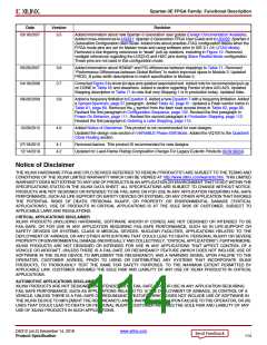
Voltage Supplies
Like Spartan-3 FPGAs, Spartan-3E FPGAs have multiple
voltage supply inputs, as shown in Table 70. There are two
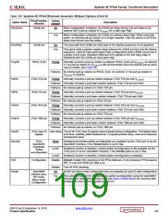
Table 70: Spartan-3E Voltage Supplies
Supply Input
Description
Nominal Supply Voltage
VCCINT
Internal core supply voltage. Supplies all internal logic functions, such as CLBs, block
RAM, and multipliers. Input to Power-On Reset (POR) circuit.
1.2V
VCCAUX
VCCO_0
VCCO_1
Auxiliary supply voltage. Supplies Digital Clock Managers (DCMs), differential drivers,
dedicated configuration pins, JTAG interface. Input to Power-On Reset (POR) circuit.
2.5V
Supplies the output buffers in I/O Bank 0, the bank along the top edge of the FPGA.
Selectable, 3.3V, 2.5V, 1.8,
1.5V, or 1.2V
Supplies the output buffers in I/O Bank 1, the bank along the right edge of the FPGA. In Selectable, 3.3V, 2.5V, 1.8,
Byte-Wide Peripheral Interface (BPI) Parallel Flash Mode, connects to the same voltage
as the Flash PROM.
1.5V, or 1.2V
VCCO_2
VCCO_3
Supplies the output buffers in I/O Bank 2, the bank along the bottom edge of the FPGA. Selectable, 3.3V, 2.5V, 1.8,
Connects to the same voltage as the FPGA configuration source. Input to Power-On
Reset (POR) circuit.
1.5V, or 1.2V
Supplies the output buffers in I/O Bank 3, the bank along the left edge of the FPGA.
Selectable, 3.3V, 2.5V, 1.8,
1.5V, or 1.2V
In a 3.3V-only application, all four V
supplies connect to
CCO
3.3V. However, Spartan-3E FPGAs provide the ability to
bridge between different I/O voltages and standards by
applying different voltages to the V
inputs of different
CCO
banks. Refer to I/O Banking Rules for which I/O standards
can be intermixed within a single I/O bank.
Each I/O bank also has an separate, optional input voltage
reference supply, called V
. If the I/O bank includes an I/O
REF
standard that requires a voltage reference such as HSTL or
SSTL, then all V pins within the I/O bank must be
REF
connected to the same voltage.
DS312 (v4.2) December 14, 2018
www.xilinx.com
Product Specification
110

 XILINX [ XILINX, INC ]