Philips Semiconductors
Preliminary specification
320 macrocell SRAM CPLD
PZ3320C/PZ3320N
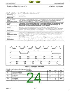
Table 7. PZ3320 Low-Level JTAG Boundary-Scan Commands
INSTRUCTION
(Instruction Code)
Register Used
DESCRIPTION
SAMPLE/PRELOAD
(00010)
Boundary-Scan Register
The mandatory SAMPLE/PRELOAD instruction allows a snapshot of the normal operation of the component
to be taken and examined. It also allows data values to be loaded onto the latched parallel outputs of the
Boundary-Scan Shift-Register prior to selection of the other boundary-scan test instructions.
EXTEST
(00000)
Boundary-Scan Register
The mandatory EXTEST instruction allows testing of off-chip circuitry and board level interconnections. Data
would typically be loaded onto the latched parallel outputs of Boundary-Scan Shift-Register using the
SAMPLE/PRELOAD instruction prior to selection of the EXTEST instruction.
BYPASS
(11111)
Bypass Register
Places the 1 bit bypass register between the tdi and tdo pins, which allows the BST data to pass
synchronously through the selected device to adjacent devices during normal device operation. The BYPASS
instruction can be entered by holding tdi at a constant high value and completing an Instruction-Scan cycle.
IDCODE
(00001)
Boundary-Scan Register
Selects the IDCODE register and places it between tdi and tdo, allowing the IDCODE to be serially shifted
out of tdo. The IDCODE instruction permits blind interrogation of the components assembled onto a printed
circuit board. Thus, in circumstances where the component population may vary, it is possible to determine
what components exist in a product.
HIGHZ
(00101)
Bypass Register
The HIGHZ instruction places the component in a state in which all of its system logic outputs are placed in
an inactive drive state (e.g., high impedance). In this state, an in-circuit test system may drive signals onto
the connections normally driven by a component output without incurring the risk of damage to the
component. The HIGHZ instruction also forces the Bypass Register between tdi and tdo.
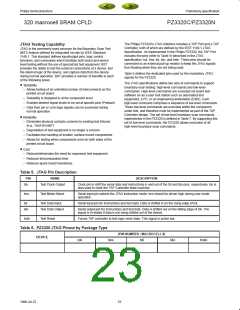
TCK
TMS
t
S
t
H
t
t
CL
CH
TDI
t
D
TDO
SP00613
Figure 29. Boundary Scan Timing Diagram
Table 8. Boundary scan timing characteristics
SYMBOL
PARAMETER
MIN
20
0
MAX
–
UNIT
t
t
t
t
f
t
tdi/tms to tck setup time
tdi/tms from tck hold time
tck high time
ns
ns
S
–
H
50
50
–
–
ns
CH
CL
TCK
D
tck low time
–
ns
tck frequency
10
20
MHz
ns
tck to tdo delay
–
24
1998 Jul 22

 XILINX [ XILINX, INC ]