Philips Semiconductors
Preliminary specification
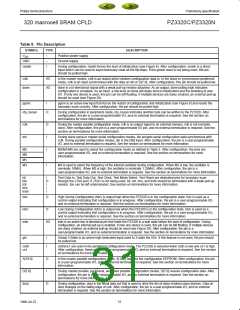
320 macrocell SRAM CPLD
PZ3320C/PZ3320N
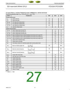
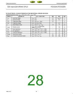
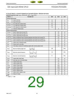
AC ELECTRICAL CHARACTERISTICS FOR COMMERCIAL GRADE DEVICES
Commercial temperature range: V = 3.0V to 3.6V; 0°C < T
< 70°C
DD
amb
SYMBOL
PARAMETER
MIN
MAX
UNIT
Timing requirements
t
t
t
t
t
t
Clock LOW time
Clock HIGH time
2.5
2.5
4.0
5.5
6.5
ns
ns
ns
ns
ns
ns
CL
CH
PAL setup time (Global clock)
PLA setup time (Global clock)
XOR setup time (Global clock)
Hold time (Global clock)
SU_PAL
SU_PLA
SU_XOR
H
0
Output characteristics
t
t
t
t
t
t
t
t
t
Input to output delay through PAL
Input to output delay through PLA
7.5
9.0
10.0
4.0
5.5
6.5
2.5
6.0
1.0
ns
ns
ns
ns
ns
ns
ns
ns
ns
PD_PAL
PD_PLA
PD_XOR
PDF_PAL
PDF_PLA
PDF_XOR
CF
Input to output delay through XOR
Input (or feedback node) to internal feedback node delay time through PAL
Input (or feedback node) to internal feedback node delay time through PLA
Input (or feedback node) to internal feedback node delay time through XOR
Global clock to feedback delay
Global clock to out delay
CO
Clock skew (variance for switching outputs with common global clock)
CS
1
f
f
f
200
154
100
MHz
MHz
MHz
ǒt Ǔ
Maximum flip-flop toggle rate
MAX1
CL ) tCH
1
ǒt
ǒt
Ǔ
Maximum internal frequency
Maximum external frequency
MAX2
SU_PAL ) tCF
1
Ǔ
MAX3
SU_PAL ) tCO
t
t
t
t
t
t
t
t
t
t
Output buffer delay (fast)
Slow slew rate incremental delay
Output enable delay
3.5
8.0
ns
ns
ns
ns
ns
ns
ns
ns
ns
ns
BUFF
SSR
EA
8.0
1
Output disable delay
8.0
ER
Global 3-State enable
Global 3-State disable
Input to register reset
Input to register preset
Global reset to register reset
Global ZIA delay
40.0
40.0
10.5
10.5
40
GTSH
GTSR
RR
RP
GRR
4.0
GZIA
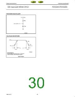
NOTE:
1. Output C = 5.0pF.
L
27
1998 Jul 22

 XILINX [ XILINX, INC ]