R
Functional Description
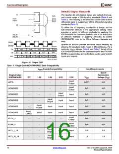
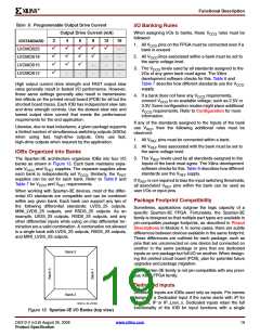
Table 8: Programmable Output Drive Current
I/O Banking Rules
Output Drive Current (mA)
When assigning I/Os to banks, these V
followed:
rules must be
CCO
2
4
ꢀ
ꢀ
ꢀ
-
6
ꢀ
ꢀ
ꢀ
-
8
ꢀ
ꢀ
-
12
ꢀ
-
16
-
IOSTANDARD
LVCMOS25
LVCMOS18
LVCMOS15
LVCMOS12
1. All V
pins on the FPGA must be connected even if a
CCO
ꢀ
ꢀ
ꢀ
ꢀ
bank is unused.
2. All V
lines associated within a bank must be set to
-
CCO
the same voltage level.
-
-
3. The V
levels used by all standards assigned to the
CCO
-
-
-
I/Os of any given bank must agree. The Xilinx
development software checks for this. Table 6 and
Table 7 describe how different standards use the V
supply.
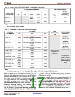
High output current drive strength and FAST output slew
rates generally result in fastest I/O performance. However,
these same settings generally also result in transmission
line effects on the printed circuit board (PCB) for all but the
shortest board traces. Each IOB has independent slew rate
and drive strength controls. Use the slowest slew rate and
lowest output drive current that meets the performance
requirements for the end application.
CCO
4. If a bank does not have any V
requirements,
CCO
connect V
to an available voltage, such as 2.5V or
CCO
3.3V. Some configuration modes might place additional
V
requirements. Refer to Configuration for more
CCO
information.
If any of the standards assigned to the Inputs of the bank
Likewise, due to lead inductance, a given package supports
a limited number of simultaneous switching outputs (SSOs)
when using fast, high-drive outputs. Only use fast,
high-drive outputs when required by the application.
use V , then the following additional rules must be
REF
observed:
1. All V
pins must be connected within a bank.
REF
2. All V
lines associated with the bank must be set to
REF
the same voltage level.
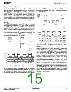
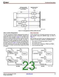
IOBs Organized into Banks
3. The V
levels used by all standards assigned to the
The Spartan-3E architecture organizes IOBs into four I/O
banks as shown in Figure 13. Each bank maintains sepa-
REF
Inputs of the bank must agree. The Xilinx development
software checks for this. Table 6 describes how different
rate V
and V
supplies. The separate supplies allow
CCO
REF
standards use the V
supply.
each bank to independently set V
. Similarly, the V
REF
REF
CCO
supplies can be set for each bank. Refer to Table 6 and
Table 7 for V and V requirements.
If V
is not required to bias the input switching thresholds,
REF
CCO
REF
all associated V
pins within the bank can be used as
REF
user I/Os or input pins.
When working with Spartan-3E devices, most of the differ-
ential I/O standards are compatible and can be combined
within any given bank. Each bank can support any two of
the following differential standards: LVDS_25 outputs,
MINI_LVDS_25 outputs, and RSDS_25 outputs. As an
example, LVDS_25 outputs, RSDS_25 outputs, and any
other differential inputs while using on-chip differential ter-
mination are a valid combination. A combination not allowed
is a single bank with LVDS_25 outputs, RSDS_25 outputs,
and MINI_LVDS_25 outputs.
Package Footprint Compatibility
Sometimes, applications outgrow the logic capacity of a
specific Spartan-3E FPGA. Fortunately, the Spartan-3E
family is designed so that multiple part types are available in
pin-compatible package footprints, as described in Pinout
Descriptions in Module 4. In some cases, there are subtle
differences between devices available in the same footprint.
These differences are outlined for each package, such as
pins that are unconnected on one device but connected on
another in the same package or pins that are dedicated
inputs on one package but full I/O on another. When design-
ing the printed circuit board (PCB), plan for potential future
upgrades and package migration.
Bank 0
The Spartan-3E family is not pin-compatible with any previ-
ous Xilinx FPGA family.
Dedicated Inputs
Dedicated Inputs are IOBs used only as inputs. Pin names
designate a Dedicated Input if the name starts with IP, for
example, IP or IP_Lxxx_x. Dedicated inputs retain the full
functionality of the IOB for input functions with a single
Bank 2
DS312-2_26_021205
Figure 13: Spartan-3E I/O Banks (top view)
DS312-2 (v3.8) August 26, 2009
www.xilinx.com
19
Product Specification

 XILINX [ XILINX, INC ]