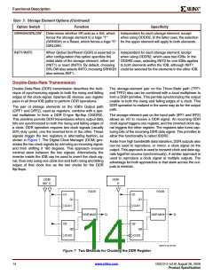
R
Functional Description
V
provides current to the outputs and additionally pow-
By default, PULLDOWN resistors terminate all unused I/O
and Input-only pins. Unused I/O and Input-only pins can
alternatively be set to PULLUP or FLOAT. To change the
unused I/O Pad setting, set the Bitstream Generator (Bit-
Gen) option UnusedPin to PULLUP, PULLDOWN, or
FLOAT. The UnusedPin option is accessed through the
Properties for Generate Programming File in ISE. See Bit-
stream Generator (BitGen) Options.
CCO
ers the On-Chip Differential Termination. V
must be
CCO
2.5V when using the On-Chip Differential Termination. The
lines are not required for differential operation.
V
REF
To further understand how to combine multiple IOSTAN-
DARDs within a bank, refer to IOBs Organized into Banks,
page 19.
On-Chip Differential Termination
During configuration a Low logic level on the HSWAP pin
activates pull-up resistors on all I/O and Input-only pins not
actively used in the selected configuration mode.
Spartan-3E devices provide an on-chip ~120Ω differential
termination across the input differential receiver terminals.
The on-chip input differential termination in Spartan-3E
devices potentially eliminates the external 100Ωtermination
resistor commonly found in differential receiver circuits. Dif-
ferential termination is used for LVDS, mini-LVDS, and
RSDS as applications permit.
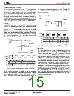
Keeper Circuit
Each I/O has an optional keeper circuit (see Figure 12) that
keeps bus lines from floating when not being actively driven.
The KEEPER circuit retains the last logic level on a line after
all drivers have been turned off. Apply the KEEPER
attribute or use the KEEPER library primitive to use the
KEEPER circuitry. Pull-up and pull-down resistors override
the KEEPER settings.
On-chip Differential Termination is available in banks with
V
= 2.5V and is not supported on dedicated input pins.
CCO
Set the DIFF_TERM attribute to TRUE to enable Differential
Termination on a differential I/O pin pair.
The DIFF_TERM attribute uses the following syntax in the
UCF file:
Pull-up
INST <I/O_BUFFER_INSTANTIATION_NAME>
DIFF_TERM = “<TRUE/FALSE>”;
Output Path
Input Path
Spartan-3E
Differential
Output
Spartan-3E
Differential Input
Z
= 50Ω
0
Keeper
Pull-down
DS312-2_25_020807
Z
Z
= 50Ω
= 50Ω
0
Figure 12: Keeper Circuit
Spartan-3E
Differential Input
with On-Chip
Differential
Slew Rate Control and Drive Strength
Spartan-3E
Differential
Output
0
Each IOB has a slew-rate control that sets the output
switching edge-rate for LVCMOS and LVTTL outputs. The
SLEW attribute controls the slew rate and can either be set
to SLOW (default) or FAST.
Terminator
Z
= 50Ω
0
Each LVCMOS and LVTTL output additionally supports up
to six different drive current strengths as shown in Table 8.
To adjust the drive strength for each output, the DRIVE
attribute is set to the desired drive strength: 2, 4, 6, 8, 12,
and 16. Unless otherwise specified in the FPGA application,
the software default IOSTANDARD is LVCMOS25, SLOW
slew rate, and 12 mA output drive.
DS312-2_24_082605
Figure 11: Differential Inputs and Outputs
Pull-Up and Pull-Down Resistors
Pull-up and pull-down resistors inside each IOB optionally
force a floating I/O or Input-only pin to a determined state.
Pull-up and pull-down resistors are commonly applied to
unused I/Os, inputs, and three-state outputs, but can be
used on any I/O or Input-only pin. The pull-up resistor con-
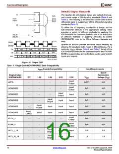
Table 8: Programmable Output Drive Current
Output Drive Current (mA)
nects an IOB to V
through a resistor. The resistance
CCO
value depends on the V
voltage (see DC and Switch-
2
4
6
8
12
ꢀ
ꢀ
16
ꢀ
ꢀ
IOSTANDARD
LVTTL
CCO
ing Characteristics in Module 3 for the specifications). The
pull-down resistor similarly connects an IOB to ground with
a resistor. The PULLUP and PULLDOWN attributes and
library primitives turn on these optional resistors.
ꢀ
ꢀ
ꢀ
ꢀ
ꢀ
ꢀ
ꢀ
ꢀ
LVCMOS33
18
www.xilinx.com
DS312-2 (v3.8) August 26, 2009
Product Specification

 XILINX [ XILINX, INC ]