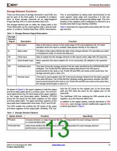
R
Functional Description
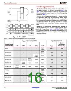
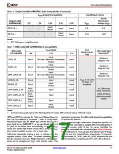
Table 6: Single-Ended IOSTANDARD Bank Compatibility (Continued)
V
Supply/Compatibility
Input Requirements
CCO
Board
Single-Ended
IOSTANDARD
Termination
1.2V
1.5V
1.8V
2.5V
3.3V
V
Voltage (V )
REF
TT
Input/
Output
SSTL18_I
-
-
Input
Input
0.9
0.9
Input/
Output
SSTL2_I
-
-
-
Input
1.25
1.25
Notes:
1. N/R - Not required for input operation.
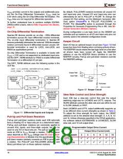
Table 7: Differential IOSTANDARD Bank Compatibility
VCCO Supply
Input
Requirements:
VREF
Differential
IOSTANDARD
Differential Bank
Restriction(1)
1.8V
2.5V
3.3V
Input,
Applies to
Outputs Only
LVDS_25
Input
On-chip Differential Termination,
Output
Input
Input,
On-chip Differential Termination,
Output
Applies to
Outputs Only
RSDS_25
Input
Input
Input
Input
Input,
On-chip Differential Termination,
Output
Applies to
Outputs Only
MINI_LVDS_25
V is not used
REF
for these I/O
standards
LVPECL_25
BLVDS_25
Input
Input
Input
Input
Input
Input,
Output
No Differential
Bank Restriction
Input,
Output
DIFF_HSTL_I_18
DIFF_HSTL_III_18
DIFF_SSTL18_I
Input
Input
Input
Input
Input
Input
Input
Input,
Output
(other I/O bank
restrictionsmight
apply)
Input,
Output
Input,
Output
DIFF_SSTL2_I
Input
Notes:
1. Each bank can support any two of the following: LVDS_25 outputs, MINI_LVDS_25 outputs, RSDS_25 outputs.
HSTL and SSTL inputs use the Reference Voltage (V
) to
subsection introduces the differential signaling capabilities
of Spartan-3E devices.
REF
bias the input-switching threshold. Once a configuration
data file is loaded into the FPGA that calls for the I/Os of a
given bank to use HSTL/SSTL, a few specifically reserved
I/O pins on the same bank automatically convert to V
inputs. For banks that do not contain HSTL or SSTL, V
pins remain available for user I/Os or input pins.
Each device-package combination designates specific I/O
pairs specially optimized to support differential standards. A
unique L-number, part of the pin name, identifies the
line-pairs associated with each bank (see Pinout Descrip-
tions in Module 4). For each pair, the letters P and N desig-
nate the true and inverted lines, respectively. For example,
the pin names IO_L43P_3 and IO_L43N_3 indicate the true
and inverted lines comprising the line pair L43 on Bank 3.
REF
REF
Differential standards employ a pair of signals, one the
opposite polarity of the other. The noise canceling proper-
ties (for example, Common-Mode Rejection) of these stan-
dards permit exceptionally high data transfer rates. This
DS312-2 (v3.8) August 26, 2009
www.xilinx.com
17
Product Specification

 XILINX [ XILINX, INC ]