R
Functional Description
exception for differential inputs (IP_Lxxx_x). For the differ-
ential Dedicated Inputs, the on-chip differential termination
is not available. To replace the on-chip differential termina-
tion, choose a differential pair that supports outputs
(IO_Lxxx_x) or use an external 100Ω termination resistor on
the board.
A Low level applied to the HSWAP input enables pull-up
resistors on user-I/O and input-only pins from power-on
throughout configuration. A High level on HSWAP disables
the pull-up resistors, allowing the I/Os to float. HSWAP con-
tains an internal pull-up resistor and defaults to High if left
floating. As soon as power is applied, the FPGA begins ini-
tializing its configuration memory. At the same time, the
FPGA internally asserts the Global Set-Reset (GSR), which
asynchronously resets all IOB storage elements to a default
Low state. Also see Pin Behavior During Configuration.
ESD Protection
Clamp diodes protect all device pads against damage from
Electro-Static Discharge (ESD) as well as excessive voltage
transients. Each I/O has two clamp diodes: one diode
Upon the completion of initialization and the beginning of
configuration, INIT_B goes High, sampling the M0, M1, and
M2 inputs to determine the configuration mode. Configura-
tion data is then loaded into the FPGA. The I/O drivers
remain in a high-impedance state (with or without pull-up
resistors, as determined by the HSWAP input) throughout
configuration.
extends P-to-N from the pad to V
and a second diode
CCO
extends N-to-P from the pad to GND. During operation,
these diodes are normally biased in the off state. These
clamp diodes are always connected to the pad, regardless
of the signal standard selected. The presence of diodes lim-
its the ability of Spartan-3E I/Os to tolerate high signal volt-
ages. The V absolute maximum rating in Table 73 of DC
and Switching Characteristics (Module 3) specifies the
voltage range that I/Os can tolerate.
IN
At the end of configuration, the GSR net is released, placing
the IOB registers in a Low state by default, unless the
loaded design reverses the polarity of their respective SR
inputs.
Supply Voltages for the IOBs
The IOBs are powered by three supplies:
The Global Three State (GTS) net is released during
Start-Up, marking the end of configuration and the begin-
ning of design operation in the User mode. After the GTS
net is released, all user I/Os go active while all unused I/Os
are pulled down (PULLDOWN). The designer can control
how the unused I/Os are terminated after GTS is released
by setting the Bitstream Generator (BitGen) option Unused-
Pin to PULLUP, PULLDOWN, or FLOAT.
1. The V
supplies, one for each of the FPGA’s I/O
CCO
banks, power the output drivers. The voltage on the
pins determines the voltage swing of the output
V
CCO
signal.
2.
3.
V
logic.
is the main power supply for the FPGA’s internal
is an auxiliary source of power, primarily to
CCINT
One clock cycle later (default), the Global Write Enable
(GWE) net is released allowing the RAM and registers to
change states. Once in User mode, any pull-up resistors
enabled by HSWAP revert to the user settings and HSWAP
is available as a general-purpose I/O. For more information
on PULLUP and PULLDOWN, see Pull-Up and Pull-Down
Resistors.
V
CCAUX
optimize the performance of various FPGA functions
such as I/O switching.
I/O and Input-Only Pin Behavior During
Power-On, Configuration, and User Mode
In this section, all behavior described for I/O pins also
applies to input-only pins and dual-purpose I/O pins that are
not actively involved in the currently-selected configuration
mode.
Behavior of Unused I/O Pins After
Configuration
By default, the Xilinx ISE development software automati-
cally configures all unused I/O pins as input pins with indi-
vidual internal pull-down resistors to GND.
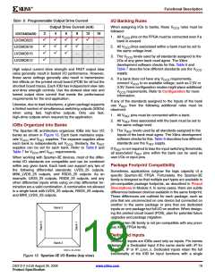
All I/O pins have ESD clamp diodes to their respective V
CCO
supply and from GND, as shown in Figure 5. The V
CCINT
(1.2V), V
(2.5V), and V
supplies can be applied in
CCAUX
CCO
This default behavior is controlled by the UnusedPin bit-
stream generator (BitGen) option, as described in Table 69.
any order. Before the FPGA can start its configuration pro-
cess, V , V Bank 2, and V must have reached
CCINT CCO
CCAUX
their respective minimum recommended operating levels
indicated in Table 74. At this time, all output drivers are in a
JTAG Boundary-Scan Capability
high-impedance state. V
serve as inputs to the internal Power-On Reset circuit
(POR).
Bank 2, V
, and V
All Spartan-3E IOBs support boundary-scan testing com-
patible with IEEE 1149.1/1532 standards. During bound-
ary-scan operations such as EXTEST and HIGHZ the
pull-down resistor is active. See JTAG Mode for more infor-
mation on programming via JTAG.
CCO
CCINT
CCAUX
20
www.xilinx.com
DS312-2 (v3.8) August 26, 2009
Product Specification

 XILINX [ XILINX, INC ]