R
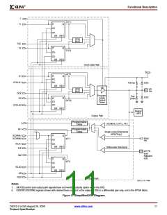
Functional Description
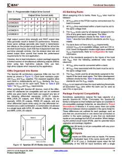
Register Cascade Feature
In the Spartan-3E family, one of the IOBs in a differential
pair can cascade its input storage elements with those in
the other IOB as part of a differential pair. This is intended to
make DDR operation at high speed much simpler to imple-
ment. The new DDR connections that are available are
shown in Figure 5 (dashed lines), and are only available for
routing between IOBs and are not accessible to the FPGA
fabric. Note that this feature is only available when using the
differential I/O standards LVDS, RSDS, and MINI_LVDS.
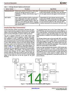
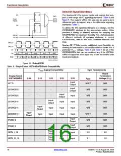
D1. Here, the FPGA fabric uses only the clock ICLK1 to pro-
cess the received data. See Figure 9 for a graphical illustra-
tion of this function.
Q
D
D1
PAD
To Fabric
D2
IDDRIN2
IQ2
Q
D
Q
D
IDDR2
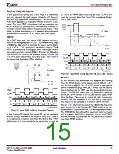
As a DDR input pair, the master IOB registers incoming
data on the rising edge of ICLK1 (= D1) and the rising edge
of ICLK2 (= D2), which is typically the same as the falling
edge of ICLK1. This data is then transferred into the FPGA
fabric. At some point, both signals must be brought into the
same clock domain, typically ICLK1. This can be difficult at
high frequencies because the available time is only one half
of a clock cycle assuming a 50% duty cycle. See Figure 8
for a graphical illustration of this function.
ICLK1
ICLK2
ICLK1
ICLK2
d
d+1 d+2 d+3 d+4 d+5 d+6 d+7 d+8
PAD
D1
d
d+2
d+1
d+4
d+3
d+6
d+5
d+8
d+7
Q
D
D1
D2
d-1
PAD
To Fabric
D2
DS312-2_22_030105
Figure 9: Input DDR Using Spartan-3E Cascade Feature
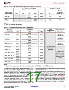
Q
D
ODDR2
As a DDR output pair, the master IOB registers data coming
from the FPGA fabric on the rising edge of OCLK1 (= D1)
and the rising edge of OCLK2 (= D2), which is typically the
same as the falling edge of OCLK1. These two bits of data
are multiplexed by the DDR mux and forwarded to the out-
put pin. The D2 data signal must be re-synchronized from
the OCLK1 clock domain to the OCLK2 domain using FPGA
slice flip-flops. Placement is critical at high frequencies,
because the time available is only one half a clock cycle.
See Figure 10 for a graphical illustration of this function.
ICLK2
ICLK1
ICLK1
ICLK2
PAD
D1
d
d+1 d+2 d+3 d+4 d+5 d+6 d+7 d+8
d+2 d+4 d+6
d
d+8
d+7
D2 d-1
d+1
d+3
d+5
The C0 or C1 alignment feature of the ODDR2 flip-flop, orig-
inally introduced in the Spartan-3E FPGA family, is not rec-
ommended or supported in the ISE development software.
The ODDR2 flip-flop without the alignment feature remains
fully supported. Without the alignment feature, the ODDR2
feature behaves equivalent to the ODDR flip-flop on previ-
ous Xilinx FPGA families.
DS312-2_21_021105
Figure 8: Input DDR (without Cascade Feature)
In the Spartan-3E device, the signal D2 can be cascaded
into the storage element of the adjacent slave IOB. There it
is re-registered to ICLK1, and only then fed to the FPGA
fabric where it is now already in the same time domain as
DS312-2 (v3.8) August 26, 2009
www.xilinx.com
15
Product Specification

 XILINX [ XILINX, INC ]