R
Functional Description
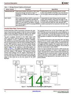
Table 5: Storage Element Options (Continued)
Option Switch
Function
Specificity
SRHIGH/SRLOW Determines whether SR acts as a Set, which
forces the storage element to a logic "1"
Independent for each storage element, except
when using ODDR2. In the latter case, the selection
(SRHIGH) or a Reset, which forces a logic "0" for the upper element will apply to both elements.
(SRLOW)
INIT1/INIT0
When Global Set/Reset (GSR) is asserted or
after configuration this option specifies the
initial state of the storage element, either set
(INIT1) or reset (INIT0). By default, choosing
Independent for each storage element, except
when using ODDR2, which uses two IOBs. In the
ODDR2 case, selecting INIT0 for one IOBs applies
to both elements within the IOB, although INIT1
SRLOW also selects INIT0; choosing SRHIGH could be selected for the elements in the other IOB.
also selects INIT1.
Double-Data-Rate Transmission
Double-Data-Rate (DDR) transmission describes the tech-
nique of synchronizing signals to both the rising and falling
edges of the clock signal. Spartan-3E devices use register
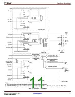
pairs in all three IOB paths to perform DDR operations.
The storage-element pair on the Three-State path (TFF1
and TFF2) also can be combined with a local multiplexer to
form a DDR primitive. This permits synchronizing the output
enable to both the rising and falling edges of a clock. This
DDR operation is realized in the same way as for the output
path.
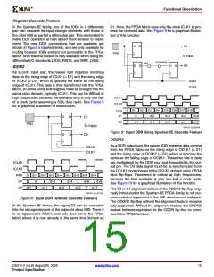
The pair of storage elements on the IOB’s Output path
(OFF1 and OFF2), used as registers, combine with a spe-
cial multiplexer to form a DDR D-type flip-flop (ODDR2).
This primitive permits DDR transmission where output data
bits are synchronized to both the rising and falling edges of
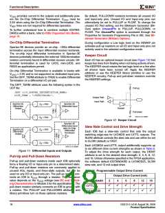
a clock. DDR operation requires two clock signals (usually
50% duty cycle), one the inverted form of the other. These
signals trigger the two registers in alternating fashion, as
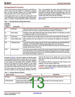
shown in Figure 7. The Digital Clock Manager (DCM) gen-
erates the two clock signals by mirroring an incoming signal,
and then shifting it 180 degrees. This approach ensures
minimal skew between the two signals. Alternatively, the
inverter inside the IOB can be used to invert the clock sig-
nal, thus only using one clock line and both rising and falling
edges of that clock line as the two clocks for the DDR
flip-flops.
The storage-element pair on the input path (IFF1 and IFF2)
allows an I/O to receive a DDR signal. An incoming DDR
clock signal triggers one register, and the inverted clock sig-
nal triggers the other register. The registers take turns cap-
turing bits of the incoming DDR data signal. The primitive to
allow this functionality is called IDDR2.
Aside from high bandwidth data transfers, DDR outputs also
can be used to reproduce, or mirror, a clock signal on the
output. This approach is used to transmit clock and data sig-
nals together (source synchronously). A similar approach is
used to reproduce a clock signal at multiple outputs. The
advantage for both approaches is that skew across the out-
puts is minimal.
DCM
DCM
0˚
180˚ 0˚
FDDR
FDDR
D1
D1
Q1
Q1
CLK1
CLK1
DDR MUX
DDR MUX
Q
Q
D2
Q2
D2
Q2
CLK2
CLK2
DS312-2_20_021105
Figure 7: Two Methods for Clocking the DDR Register
14
www.xilinx.com
DS312-2 (v3.8) August 26, 2009
Product Specification

 XILINX [ XILINX, INC ]