R
Functional Description
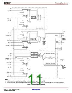
Input Delay Functions
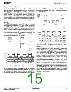
Each IOB has a programmable delay block that optionally
delays the input signal. In Figure 6, the signal path has a
coarse delay element that can be bypassed. The input sig-
nal then feeds a 6-tap delay line. The coarse and tap delays
vary; refer to timing reports for specific delay values. All six
taps are available via a multiplexer for use as an asynchro-
nous input directly into the FPGA fabric. In this way, the
delay is programmable in 12 steps. Three of the six taps are
also available via a multiplexer to the D inputs of the syn-
chronous storage elements. The delay inserted in the path
to the storage element can be varied in six steps. The first,
coarse delay element is common to both asynchronous and
synchronous paths, and must be either used or not used for
both paths.
generated by the implementation tools, and the resulting
effects on input timing are reported using the Timing Ana-
lyzer tool.
If the design uses a DCM in the clock path, then the delay
element can be safely set to zero because the
Delay-Locked Loop (DLL) compensation automatically
ensures that there is still no input hold time requirement.
Both asynchronous and synchronous values can be modi-
fied, which is useful where extra delay is required on clock
or data inputs, for example, in interfaces to various types of
RAM.
These delay values are defined through the
IBUF_DELAY_VALUE and the IFD_DELAY_VALUE param-
eters. The default IBUF_DELAY_VALUE is 0, bypassing the
delay elements for the asynchronous input. The user can
set this parameter to 0-12. The default IFD_DELAY_VALUE
is AUTO. IBUF_DELAY_VALUE and IFD_DELAY_VALUE
are independent for each input. If the same input pin uses
both registered and non-registered input paths, both param-
eters can be used, but they must both be in the same half of
the total delay (both either bypassing or using the coarse
delay element).
The delay values are set up in the silicon once at configura-
tion time—they are non-modifiable in device operation.
The primary use for the input delay element is to adjust the
input delay path to ensure that there is no hold time require-
ment when using the input flip-flop(s) with a global clock.
The default value is chosen automatically by the Xilinx soft-
ware tools as the value depends on device size and the spe-
cific device edge where the flip-flop resides. The value set
by the Xilinx ISE software is indicated in the Map report
IFD_DELAY_VALUE
Synchronous input (IQ1)
D Q
Synchronous input (IQ2)
D Q
Coarse Delay
PAD
Asynchronous input (I)
IBUF_DELAY_VALUE
UG331_c10_09_011508
Figure 6: Programmable Fixed Input Delay Elements
12
www.xilinx.com
DS312-2 (v3.8) August 26, 2009
Product Specification

 XILINX [ XILINX, INC ]