R
Functional Description
an output path. The following paragraphs assume that any
reference to output functionality does not apply to the
input-only blocks. The number of input-only blocks varies
with device size, but is never more than 25% of the total IOB
count.
Introduction
As described in Architectural Overview, the Spartan™-3E
FPGA architecture consists of five fundamental functional
elements:
•
•
Input/Output Blocks (IOBs)
Configurable Logic Block (CLB) and Slice
Resources
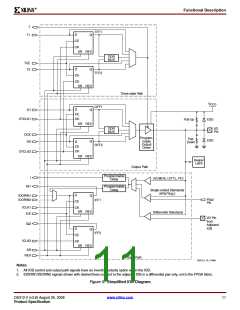
Figure 5, page 11 is a simplified diagram of the IOB’s inter-
nal structure. There are three main signal paths within the
IOB: the output path, input path, and 3-state path. Each
path has its own pair of storage elements that can act as
either registers or latches. For more information, see Stor-
age Element Functions. The three main signal paths are
as follows:
•
•
•
Block RAM
Dedicated Multipliers
Digital Clock Managers (DCMs)
The following sections provide detailed information on each
of these functions. In addition, this section also describes
the following functions:
•
The input path carries data from the pad, which is
bonded to a package pin, through an optional
programmable delay element directly to the I line. After
the delay element, there are alternate routes through a
pair of storage elements to the IQ1 and IQ2 lines. The
IOB outputs I, IQ1, and IQ2 lead to the FPGA’s internal
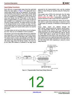
logic. The delay element can be set to ensure a hold
time of zero (see Input Delay Functions).
•
•
•
•
Clocking Infrastructure
Interconnect
Configuration
Powering Spartan-3E FPGAs
•
•
The output path, starting with the O1 and O2 lines,
carries data from the FPGA’s internal logic through a
multiplexer and then a three-state driver to the IOB
pad. In addition to this direct path, the multiplexer
provides the option to insert a pair of storage elements.
The 3-state path determines when the output driver is
high impedance. The T1 and T2 lines carry data from
the FPGA’s internal logic through a multiplexer to the
output driver. In addition to this direct path, the
multiplexer provides the option to insert a pair of
storage elements.
Input/Output Blocks (IOBs)
For additional information, refer to the “Using I/O
Resources” chapter in UG331.
IOB Overview
The Input/Output Block (IOB) provides a programmable,
unidirectional or bidirectional interface between a package
pin and the FPGA’s internal logic. The IOB is similar to that
of the Spartan-3 family with the following differences:
•
•
•
Input-only blocks are added
Programmable input delays are added to all blocks
DDR flip-flops can be shared between adjacent IOBs
•
All signal paths entering the IOB, including those
associated with the storage elements, have an inverter
option. Any inverter placed on these paths is
automatically absorbed into the IOB.
The unidirectional input-only block has a subset of the full
IOB capabilities. Thus there are no connections or logic for
10
www.xilinx.com
DS312-2 (v3.8) August 26, 2009
Product Specification

 XILINX [ XILINX, INC ]