Spartan-6 FPGA Data Sheet: DC and Switching Characteristics
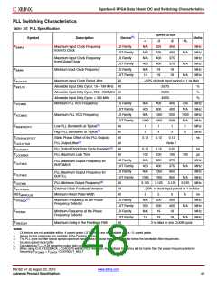
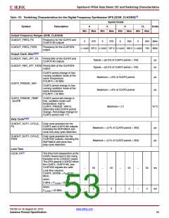
Table 52: Switching Characteristics for the Delay-Locked Loop (DLL)(1) (Cont’d)
Speed Grade
-3 -2
Min Max Min Max Min Max Min Max
Symbol
Description
-4
-1L
Units
LOCK_DLL(3)
When using the DLL alone: The time
from deassertion at the DCM’s reset
input to the rising transition at its
LOCKED output. When the DCM is
locked, the CLKIN and CLKFB
signals are in phase.
–
5
–
5
–
5
–
5
ms
5 MHz < CLKIN_FREQ_DLL
< 50 MHz.
When using the DLL alone: The time
from deassertion at the DCM’s reset
input to the rising transition at its
LOCKED output. When the DCM is
locked, the CLKIN and CLKFB
signals are in phase.
–
0.60
40
–
0.60
40
–
0.60
40
–
0.60
40
ms
ps
CLKIN_FREQ_DLL > 50 MHz
Delay Lines
DCM_DELAY_STEP(5)
Finest delay resolution, averaged
over all steps.
10
10
10
10
Notes:
1. The values in this table are based on the operating conditions described in Table 2 and Table 51.
2. Indicates the maximum amount of output jitter that the DCM adds to the jitter on the CLKIN input.
3. For optimal jitter tolerance and faster LOCK time, use the CLKIN_PERIOD attribute.
4. Some jitter and duty-cycle specifications include 1% of input clock period or 0.01 UI. For example, this data sheet specifies a maximum jitter of
(1% of CLKIN period + 150 ps). Assuming that the CLKIN frequency is 100 MHz, the equivalent CLKIN period is 10 ns. Since 1% of 10 ns is 0.1 ns
or 100 ps, the maximum jitter is (100 ps + 150 ps) = 250 ps.
5. A typical delay step size is 23 ps.
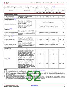
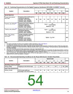
Table 53: Recommended Operating Conditions for the Digital Frequency Synthesizer (DFS)(1)
Speed Grade
Symbol
Description
-4
-3
-2
-1L
Units
Min Max Min Max Min Max Min Max
(2)
Input Frequency Ranges
CLKIN_FREQ_FX
Frequency for the CLKIN input. Also
0.5
–
375
300
0.5
–
375
300
0.5
–
333
300
MHz
ps
described as FCLKIN
.
(3)
Input Clock Jitter Tolerance
CLKIN_CYC_JITT_FX_LF Cycle-to-cycle jitter at the CLKIN input,
based on CLKFX output frequency:
–
300
FCLKFX < 150 MHz.
CLKIN_CYC_JITT_FX_HF Cycle-to-cycle jitter at the CLKIN input,
based on CLKFX output frequency:
–
–
150
1
–
–
150
1
–
–
150
1
–
–
150
1
ps
ns
FCLKFX > 150 MHz.
CLKIN_PER_JITT_FX
Period jitter at the CLKIN input.
Notes:
1. DFS specifications apply when using either of the DFS outputs (CLKFX or CLKFX180).
2. When using both DFS and DLL outputs on the same DCM, follow the more restrictive CLKIN_FREQ_DLL specifications in Table 51.
3. CLKIN input jitter beyond these limits can cause the DCM to lose LOCK.
DS162 (v1.9) August 23, 2010
www.xilinx.com
Advance Product Specification
51

 XILINX [ XILINX, INC ]