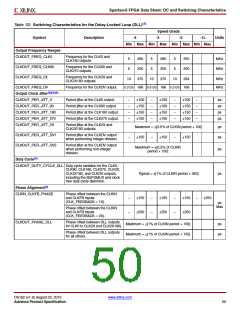
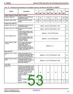
Spartan-6 FPGA Data Sheet: DC and Switching Characteristics
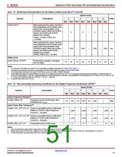
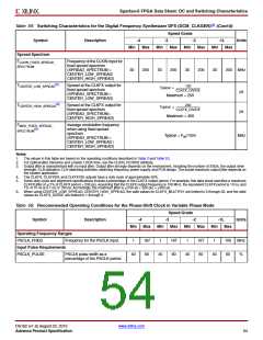
Table 55: Switching Characteristics for the Digital Frequency Synthesizer DFS (DCM_CLKGEN)(1) (Cont’d)
Speed Grade
Symbol
Description
-4
-3
-2
-1L
Units
Min
Max
Min
Max
Min
Max
Min
Max
Spread Spectrum
FCLKIN_FIXED_SPREAD_
SPECTRUM
Frequency of the CLKIN input for
fixed spread spectrum
(SPREAD_SPECTRUM =
CENTER_LOW_SPREAD/
CENTER_HIGH_SPREAD)
30
200
30
200
30
200
30
200 MHz
(6)
TCENTER_LOW_SPREAD
TCENTER_HIGH_SPREAD
FMOD_FIXED_SPREAD_
Spread at the CLKFX output for
fixed spread spectrum
(SPREAD_SPECTRUM =
CENTER_LOW_SPREAD)
100
Typical = ------------------------------------------
CLKFX_DIVIDE
ps
ps
Maximum = 250
(6)
Spread at the CLKFX output for
fixed spread spectrum
(SPREAD_SPECTRUM=
CENTER_HIGH_SPREAD)
240
Typical = ------------------------------------------
CLKFX_DIVIDE
Maximum = 400
Average modulation frequency
when using fixed spread
spectrum
(SPREAD_SPECTRUM =
CENTER_LOW_SPREAD /
CENTER_HIGH_SPREAD)
(6)
SPECTRUM
Typical = FIN/1024
MHz
Notes:
1. The values in this table are based on the operating conditions described in Table 2 and Table 53.
2. For optimal jitter tolerance and a faster LOCK time, use the CLKIN_PERIOD attribute.
3. Output jitter is characterized with no input jitter. Output jitter strongly depends on the environment, including the number of SSOs, the output drive
strength, CLB utilization, CLB switching activities, switching frequency, power supply, and PCB design. The actual maximum output jitter depends on
the system application.
4. The CLKFX, CLKFXDV, and CLKFX180 outputs have a duty cycle of approximately 50%.
5. Some duty-cycle and alignment specifications include a percentage of the CLKFX output period. For example, this data sheet specifies a maximum
CLKFX jitter of (1% of CLKFX period + 200 ps). Assuming that the CLKFX output frequency is 100 MHz, the equivalent CLKFX period is 10 ns, and
1% of 10 ns is 0.1 ns or 100 ps. Accordingly, the maximum jitter is (100 ps + 200 ps) = 300 ps.
6. When using CENTER_LOW_SPREAD, CENTER_HIGH_SPREAD, the valid values for CLKFX_MULTIPLY are limited to 2 through 32, and the valid
values for CLKFX_DIVIDE are limited to 1 through 4.
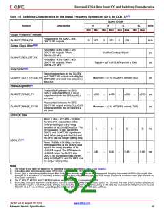
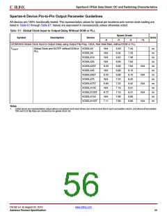
Table 56: Recommended Operating Conditions for the Phase-Shift Clock in Variable Phase Mode
Speed Grade
Symbol
Description
-4
-3
-2
-1L
Units
Min
1
Max
167
60
Min
1
Max
167
60
Min
1
Max
167
60
Min
1
Max
100
60
Operating Frequency Ranges
PSCLK_FREQ
Frequency for the PSCLK input.
MHz
%
Input Pulse Requirements
PSCLK_PULSE
PSCLK pulse width as a
40
40
40
40
percentage of the PSCLK period.
DS162 (v1.9) August 23, 2010
www.xilinx.com
Advance Product Specification
54

 XILINX [ XILINX, INC ]