Spartan-6 FPGA Data Sheet: DC and Switching Characteristics
DCM Switching Characteristics
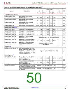
Table 51: Operating Frequency Ranges and Conditions for the Delay-Locked Loop (DLL)(1)
Speed Grade
Symbol
Description
-4
-3
-2
-1L
Min Max
Units
Min
Max
Min
Max
Min
Max
Input Frequency Ranges
CLKIN_FREQ_DLL
Frequency of the CLKIN clock
input. Also described as FCLKIN
5(2) 280(3) 5(2) 280(3) 5(2) 250(3) 5(2) 175(3) MHz
.
Input Pulse Requirements
CLKIN_PULSE
CLKIN pulse width as a
percentage of the CLKIN period
for
40
45
60
55
40
45
60
55
40
45
60
55
40
45
60
55
%
%
CLKIN_FREQ_DLL < 150 MHz
CLKIN pulse width as a
percentage of the CLKIN period
for
CLKIN_FREQ_DLL > 150 MHz
Input Clock Jitter Tolerance and Delay Path Variation(4)
CLKIN_CYC_JITT_DLL_LF Cycle-to-cycle jitter at the CLKIN
input for
CLKIN_FREQ_DLL < 150 MHz
–
–
300
150
–
–
300
150
–
–
300
150
–
–
300
150
ps
ps
CLKIN_CYC_JITT_DLL_HF
Cycle-to-cycle jitter at the CLKIN
input for
CLKIN_FREQ_DLL > 150 MHz.
CLKIN_PER_JITT_DLL
Period jitter at the CLKIN input.
–
–
1
1
–
–
1
1
–
–
1
1
–
–
1
1
ns
ns
CLKFB_DELAY_VAR_EXT
Allowable variation of the off-chip
feedback delay from the DCM
output to the CLKFB input.
Notes:
1. DLL specifications apply when using any of the DLL outputs: CLK0, CLK90, CLK180, CLK270, CLK2X, CLK2X180, or CLKDV.
2. When operating independently of the DLL, the DFS supports lower CLKIN_FREQ_DLL frequencies. See Table 53.
3. The CLKIN_DIVIDE_BY_2 attribute can be used to increase the effective input frequency range up to the F
for the global clock BUFG, see
MAX
Table 47. When set to TRUE, the CLKIN_DIVIDE_BY_2 attribute divides the incoming clock frequency by two as it enters the DCM.
4. CLKIN_FREQ_DLL input jitter beyond these limits can cause the DCM to lose LOCK, indicated by the LOCKED output deasserting. The user must
then reset the DCM.
5. When using both DCMs in a CMT, both DCMs must be LOCKED.
DS162 (v1.9) August 23, 2010
www.xilinx.com
Advance Product Specification
49

 XILINX [ XILINX, INC ]