Spartan-6 FPGA Data Sheet: DC and Switching Characteristics
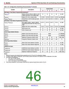
Table 52: Switching Characteristics for the Delay-Locked Loop (DLL)(1)
Speed Grade
-3 -2
Min Max Min Max Min Max Min Max
Symbol
Description
-4
-1L
Units
Output Frequency Ranges
CLKOUT_FREQ_CLK0
Frequency for the CLK0 and
CLK180 outputs.
5
5
280
200
375
5
5
280
200
375
5
5
250
200
334
MHz
MHz
CLKOUT_FREQ_CLK90
CLKOUT_FREQ_2X
CLKOUT_FREQ_DV
Frequency for the CLK90 and
CLK270 outputs.
Frequency for the CLK2X and
CLK2X180 outputs.
10
10
10
MHz
MHz
Frequency for the CLKDV output.
0.3125 186 0.3125 186 0.3125 166
(2)(3)(4)
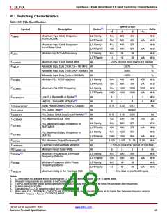
Output Clock Jitter
CLKOUT_PER_JITT_0
CLKOUT_PER_JITT_90
CLKOUT_PER_JITT_180
CLKOUT_PER_JITT_270
CLKOUT_PER_JITT_2X
Period jitter at the CLK0 output.
Period jitter at the CLK90 output.
Period jitter at the CLK180 output.
Period jitter at the CLK270 output.
–
–
–
–
100
150
150
150
–
–
–
–
100
150
150
150
–
–
–
–
100
150
150
150
–
–
–
–
ps
ps
ps
ps
Period jitter at the CLK2X and
CLK2X180 outputs.
Maximum = [0.5% of CLKIN period + 100]
150 150 150
ps
ps
CLKOUT_PER_JITT_DV1
CLKOUT_PER_JITT_DV2
Period jitter at the CLKDV output
when performing integer division.
–
–
–
Period jitter at the CLKDV output
when performing non-integer
division.
Maximum = [0.5% of CLKIN
period + 100]
ps
(4)
Duty Cycle
CLKOUT_DUTY_CYCLE_DLL Duty cycle variation for the CLK0,
CLK90, CLK180, CLK270, CLK2X,
CLK2X180, and CLKDV outputs,
Typical = [1% of CLKIN period + 350]
ps
including the BUFGMUX and clock
tree duty-cycle distortion.
(4)
Phase Alignment
CLKIN_CLKFB_PHASE
Phase offset between the CLKIN
and CLKFB inputs
(CLK_FEEDBACK = 1X).
–
–
150
250
–
–
150
250
–
–
150
250
–
250
ps
Max
Phase offset between the CLKIN
and CLKFB inputs
(CLK_FEEDBACK = 2X).
CLKOUT_PHASE_DLL
Phase offset between DLL outputs
for CLK0 to CLK2X (not CLK2X180).
Maximum = [1% of CLKIN period + 100]
Maximum = [1% of CLKIN period + 150]
ps
ps
Phase offset between DLL outputs
for all others.
DS162 (v1.9) August 23, 2010
www.xilinx.com
Advance Product Specification
50

 XILINX [ XILINX, INC ]