Spartan-6 FPGA Data Sheet: DC and Switching Characteristics
Table 57: Switching Characteristics for the Phase-Shift Clock in Variable Phase Mode(1)
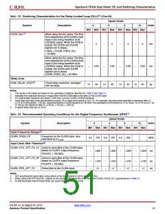
Symbol
Description
Amount of Phase Shift
Units
Phase Shifting Range
When CLKIN < 60 MHz, the maximum allowed
number of DCM_DELAY_STEP steps for a
given CLKIN clock period, where T = CLKIN
clock period in ns. When using
(INTEGER(10 x (TCLKIN – 3 ns)))
steps
CLKIN_DIVIDE_BY_2 = TRUE, double the
clock-effective clock period.
MAX_STEPS(2)
When CLKIN ≥ 60 MHz, the maximum allowed
number of DCM_DELAY_STEP steps for a
given CLKIN clock period, where T = CLKIN
clock period in ns. When using
(INTEGER(15 x (TCLKIN – 3 ns)))
steps
CLKIN_DIVIDE_BY_2 = TRUE, double the
clock-effective clock period.
Minimum guaranteed delay for variable phase
shifting.
(MAX_STEPS x DCM_DELAY_STEP_MIN)
(MAX_STEPS x DCM_DELAY_STEP_MAX)
ns
ns
FINE_SHIFT_RANGE_MIN
Maximum guaranteed delay for variable phase
shifting
FINE_SHIFT_RANGE_MAX
Notes:
1. The values in this table are based on the operating conditions described in Table 51 and Table 56.
2. The maximum variable phase shift range, MAX_STEPS, is only valid when the DCM has no initial fixed-phase shifting, that is, the PHASE_SHIFT
attribute is set to 0.
3. The DCM_DELAY_STEP values are provided at the end of Table 52.
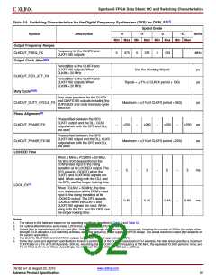
Table 58: Miscellaneous DCM Timing Parameters(1)
Symbol
Description
Min
Max
Units
DCM_RST_PW_MIN
Minimum duration of a RST pulse width
3
–
CLKIN cycles
Notes:
1. This limit only applies to applications that use the DCM DLL outputs (CLK0, CLK90, CLK180, CLK270, CLK2X, CLK2X180, and CLKDV). The DCM
DFS outputs (CLKFX, CLKFXDV, CLKFX180) are unaffected.
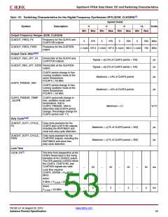
Table 59: Frequency Synthesis
Attribute
CLKFX_MULTIPLY (DCM_SP)
Min
2
Max
32
CLKFX_DIVIDE (DCM_SP)
1
32
CLKDV_DIVIDE (DCM_SP)
1.5
2
16
CLKFX_MULTIPLY (DCM_CLKGEN)
CLKFX_DIVIDE (DCM_CLKGEN)
CLKFXDV_DIVIDE (DCM_CLKGEN)
256
256
32
1
2
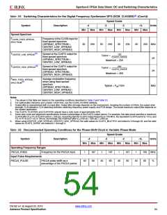
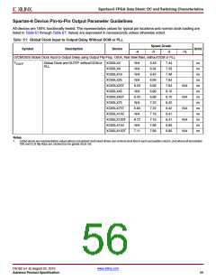
Table 60: DCM Switching Characteristics
Symbol
Speed Grade
Description
PSEN Setup/Hold
Units
-4
-3
-2
-1L
TDMCCK_PSEN/ TDMCKC_PSEN
1.50
0.00
1.50
0.00
1.50
0.00
1.50
0.00
ns
TDMCCK_PSINCDEC/ TDMCKC_PSINCDEC
TDMCKO_PSDONE
PSINCDEC Setup/Hold
Clock to out of PSDONE
1.50
0.00
1.50
0.00
1.50
0.00
1.50
0.00
ns
ns
1.50
1.50
1.50
1.50
DS162 (v1.9) August 23, 2010
www.xilinx.com
Advance Product Specification
55

 XILINX [ XILINX, INC ]