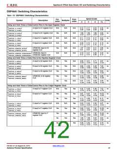
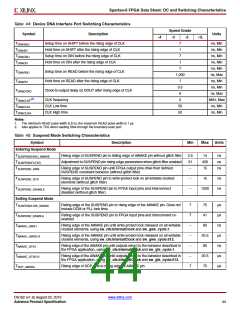
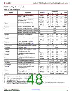
Spartan-6 FPGA Data Sheet: DC and Switching Characteristics
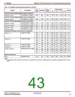
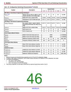
Table 46: Configuration Switching Characteristics(1) (Cont’d)
Speed Grade
Symbol
Description
Units
-4
-3
-2
-1L
BPI Master Flash Mode Programming Switching(3)
(4)
TBPICCO
A[25:0], FCS_B, FOE_B, FWE_B, LDC
outputs valid after CCLK falling edge
15
15
15
20
ns, Min
TBPIICCK
Master BPI CCLK (output) delay
10/100 10/100 10/100 10/130 µs, Min/Max
TBPIDCC/TBPICCD
Setup/Hold on D[15:0] data input pins
5.0/1.0 5.0/1.0 5.0/1.0 6.0/2.0
ns, Min
SPI Master Flash Mode Programming Switching
T
SPIDCC/TSPIDCCD
DIN, MISO0, MISO1, MISO2, MISO3,
Setup/Hold before/after the rising CCLK
edge
5.0/1.0 5.0/1.0 5.0/1.0 7.0/1.0
ns, Min
TSPIICCK
Master SPI CCLK (output) delay
MOSI clock to out
0.4/7.0 0.4/7.0 0.4/7.0 0.4/10.0 µs, Min/Max
TSPICCM
13
16
13
16
13
16
19
26
ns, Max
ns, Max
TSPICCFC
CSO_B clock to out
CCLK Output (Master Modes)
TMCCKL
Master CCLK clock duty cycle Low
Master CCLK clock duty cycle High
Maximum Frequency, master mode
Frequency Tolerance, master mode
40/60
40/60
%, Min/Max
%, Min/Max
MHz, Max
%
TMCCKH
FMCCK
40
50
40
40
30
FMCCKTOL
50
50
50
CCLK Input (Slave Modes)
TSCCKL
Slave CCLK clock minimum Low time
Slave CCLK clock minimum High time
5
5
5
5
5
5
8
8
ns, Min
ns, Min
TSCCKH
USERCCLK Input
TUSERCCLKL
TUSERCCLKH
FUSERCCLK
USERCCLK clock minimum Low time
USERCCLK clock minimum High time
Maximum USERCCLK frequency
12
12
40
12
12
40
12
12
40
21
21
30
ns, Min
ns, Min
MHz, Max
Notes:
1. Maximum frequency and setup/hold timing parameters are for 3.3V and 2.5V configuration voltages.
2. To support longer delays in configuration, use the design solutions described in the Spartan-6 FPGA Configuration User Guide.
3. BPI mode is not supported in:
•
•
•
LX4, LX25, or LX25T devices
LX9 devices in the TQG144 package
LX9 or LX16 devices in the CPG196 package.
4. Only during configuration, the last edge is determined by a weak pull-up/pull-down resistor in the I/O.
DS162 (v1.9) August 23, 2010
www.xilinx.com
Advance Product Specification
46

 XILINX [ XILINX, INC ]