R
Platform Flash In-System Programmable Configuration PROMs
Table 12: XCFxxS Pin Names and Descriptions (Cont’d)
Boundary
Scan Order
Boundary-Scan
Function
20-pin TSSOP
(VO20/VOG20)
Pin Name
Pin Description
JTAG Serial Data Output. This pin is the serial output for all
JTAG instruction and data registers. TDO has an internal
50 kΩ resistive pull-up to VCCJ to provide a logic 1 to the
system if the pin is not driven.
TDO
–
Data Out
17
VCCINT
VCCO
–
–
–
–
+3.3V Supply. Positive 3.3V supply voltage for internal logic.
18
19
+3.3V, 2.5V, or 1.8V I/O Supply. Positive 3.3V, 2.5V, or 1.8V
supply voltage connected to the output voltage drivers and
input buffers.
+3.3V or 2.5V JTAG I/O Supply. Positive 3.3V or 2.5V supply
voltage connected to the TDO output voltage driver and TCK,
TMS, and TDI input buffers.
VCCJ
–
–
20
GND
DNC
–
–
–
–
Ground
11
Do not connect. (These pins must be left unconnected.)
2, 9, 12, 14, 15, 16
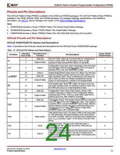
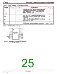
XCFxxS VO20/VOG20 Pinout Diagram
X-Ref Target - Figure 11
1
2
3
4
5
6
7
8
9
20
19
18
17
16
15
14
13
12
11
D0
(DNC)
CLK
VCCJ
VCCO
VCCINT
TDO
TDI
VO20/VOG20
Top View
TMS
(DNC)
(DNC)
(DNC)
CEO
TCK
CF
OE/RESET
(DNC)
CE
(DNC)
GND
10
ds123_02_071304
Figure 11: VO20/VOG20 Pinout Diagram (Top View)
with Pin Names
DS123 (v2.18) May 19, 2010
www.xilinx.com
Product Specification
25

 XILINX [ XILINX, INC ]