R
Platform Flash In-System Programmable Configuration PROMs
Pinouts and Pin Descriptions
The XCFxxS Platform Flash PROM is available in the VO20 and VOG20 packages. The XCFxxP Platform Flash PROM is
available in the VO48, VOG48, FS48, and FSG48 packages. For package drawings, specifications, and additional
information, see UG112, Device Package User Guide, or the Xilinx Package Specifications.
Note:
1. VO20/VOG20 denotes a 20-pin (TSSOP) Plastic Thin Shrink Small Outline Package.
2. VO48/VOG48 denotes a 48-pin (TSOP) Plastic Thin Small Outline Package.
3. FS48/FSG48 denotes a 48-pin (TFBGA) Plastic Thin Fine Pitch Ball Grid Array (0.8 mm pitch).
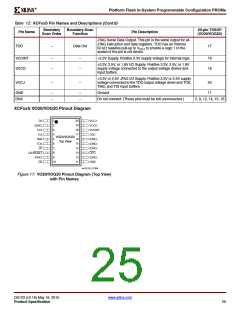
XCFxxS Pinouts and Pin Descriptions
XCFxxS VO20/VOG20 Pin Names and Descriptions
Table 12 provides a list of the pin names and descriptions for the XCFxxS 20-pin VO20/VOG20 package.
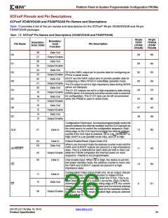
Table 12: XCFxxS Pin Names and Descriptions
Boundary
Scan Order
Boundary-Scan
Function
20-pin TSSOP
(VO20/VOG20)
Pin Name
Pin Description
4
3
Data Out
D0 is the DATA output pin to provide data for configuring an
FPGA in serial mode. The D0 output is set to a high-
impedance state during ISPEN (when not clamped).
D0
1
3
Output Enable
Configuration Clock Input. Each rising edge on the CLK input
increments the internal address counter if the CLK input is
selected, CE is Low, and OE/RESET is High.
CLK
0
Data In
20
19
Data In
Output Enable/Reset (Open-Drain I/O). When Low, this input
holds the address counter reset and the DATA output is in a
high-impedance state. This is a bidirectional open-drain pin
that is held Low while the PROM completes the internal
power-on reset sequence. Polarity is not programmable.
Data Out
OE/RESET
8
18
Output Enable
Chip Enable Input. When CE is High, the device is put into
low-power standby mode, the address counter is reset, and
the DATA pins are put in a high-impedance state.
CE
CF
15
Data In
10
7
22
21
12
Data Out
Output Enable
Data Out
Configuration Pulse (Open-Drain Output). Allows JTAG
CONFIG instruction to initiate FPGA configuration without
powering down FPGA. This is an open-drain output that is
pulsed Low by the JTAG CONFIG command.
Chip Enable Output. Chip Enable Output (CEO) is connected
to the CE input of the next PROM in the chain. This output is
Low when CE is Low and OE/RESET input is High, AND the
internal address counter has been incremented beyond its
Terminal Count (TC) value. CEO returns to High when
OE/RESET goes Low or CE goes High.
CEO
TMS
13
5
11
–
Output Enable
Mode Select
JTAG Mode Select Input. The state of TMS on the rising edge
of TCK determines the state transitions at the Test Access
Port (TAP) controller. TMS has an internal 50 kΩ resistive pull-
up to VCCJ to provide a logic 1 to the device if the pin is not
driven.
JTAG Clock Input. This pin is the JTAG test clock. It
sequences the TAP controller and all the JTAG test and
programming electronics.
TCK
TDI
–
–
Clock
6
4
JTAG Serial Data Input. This pin is the serial input to all JTAG
instruction and data registers. TDI has an internal 50 kΩ
resistive pull-up to VCCJ to provide a logic 1 to the device if the
pin is not driven.
Data In
DS123 (v2.18) May 19, 2010
www.xilinx.com
Product Specification
24

 XILINX [ XILINX, INC ]