R
Platform Flash In-System Programmable Configuration PROMs
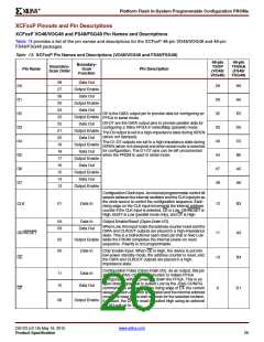
Table 13: XCFxxP Pin Names and Descriptions (VO48/VOG48 and FS48/FSG48) (Cont’d)
48-pin
TSOP
(VO48/
VOG48)
48-pin
TFBGA
(FS48/
FSG48)
Boundary-
Boundary-
Pin Name
Scan
Pin Description
Scan Order
Function
06
Data Out
Chip Enable Output. Chip Enable Output (CEO) is connected
to the CE input of the next PROM in the chain. This output is
Low when CE is Low and OE/RESET input is High, AND the
internal address counter has been incremented beyond its
Terminal Count (TC) value or the PROM does not contain any
blocks that correspond to the selected revision. CEO returns
to High when OE/RESET goes Low or CE goes High.
CEO
10
25
D2
H4
05
31
Output Enable
Enable External Selection Input. When this pin is Low, design
revision selection is controlled by the Revision Select pins.
When this pin is High, design revision selection is controlled
by the internal programmable Revision Select control bits.
EN_EXT_SEL has an internal 50 kΩ resistive pull-up to
EN_EXT_SEL
Data In
VCCO to provide a logic 1 to the device if the pin is not driven.
REV_SEL0
REV_SEL1
30
29
Data In
Data In
Revision Select[1:0] Inputs. When the EN_EXT_SEL is Low,
the Revision Select pins are used to select the design
revision to be enabled, overriding the internal programmable
Revision Select control bits. The Revision Select[1:0] inputs
have an internal 50 kΩ resistive pull-up to VCCO to provide a
logic 1 to the device if the pins are not driven.
26
27
G3
G4
Busy Input. The BUSY input is enabled when parallel mode
is selected for configuration. When BUSY is High, the internal
address counter stops incrementing and the current data
remains on the data pins. On the first rising edge of CLK after
BUSY transitions from High to Low, the data for the next
address is driven on the data pins. When serial mode or
decompression is enabled during device programming, the
BUSY input is disabled. BUSY has an internal 50 kΩ resistive
pull-down to GND to provide a logic 0 to the device if the pin
is not driven.
BUSY
12
08
Data In
5
C1
Data Out
Configuration Clock Output. An internal Programmable
control bit enables the CLKOUT signal, which is sourced from
either the internal oscillator or the CLK input pin. Each rising
edge of the selected clock source increments the internal
address counter if data is available, CE is Low, and
OE/RESET is High. Output data is available on the rising
edge of CLKOUT. CLKOUT is disabled if CE is High or
OE/RESET is Low. If decompression is enabled, CLKOUT is
parked High when decompressed data is not ready. When
CLKOUT is disabled, the CLKOUT pin is put into a high-Z
state. If CLKOUT is used, then it must be pulled High
CLKOUT
9
C2
07
Output Enable
externally using a 4.7 kΩ pull-up to VCCO
.
JTAG Mode Select Input. The state of TMS on the rising edge
of TCK determines the state transitions at the Test Access Port
(TAP) controller. TMS has an internal 50 kΩ resistive pull-up to
VCCJ to provide a logic 1 to the device if the pin is not driven.
TMS
TCK
TDI
–
–
–
Mode Select
Clock
21
20
19
E2
H3
G1
JTAG Clock Input. This pin is the JTAG test clock. It
sequences the TAP controller and all the JTAG test and
programming electronics.
JTAG Serial Data Input. This pin is the serial input to all JTAG
instruction and data registers. TDI has an internal 50 kΩ
resistive pull-up to VCCJ to provide a logic 1 to the device if
the pin is not driven.
Data In
JTAG Serial Data Output. This pin is the serial output for all
JTAG instruction and data registers. TDO has an internal
50 kΩ resistive pull-up to VCCJ to provide a logic 1 to the
system if the pin is not driven.
TDO
–
Data Out
22
E6
DS123 (v2.18) May 19, 2010
www.xilinx.com
Product Specification
27

 XILINX [ XILINX, INC ]