R
Platform Flash In-System Programmable Configuration PROMs
XCFxxP Pinouts and Pin Descriptions
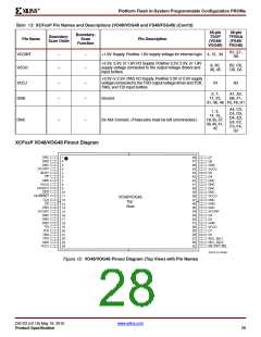
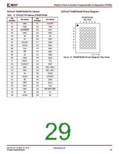
XCFxxP VO48/VOG48 and FS48/FSG48 Pin Names and Descriptions
Table 13 provides a list of the pin names and descriptions for the XCFxxP 48-pin VO48/VOG48 and 48-pin
FS48/FSG48 packages.
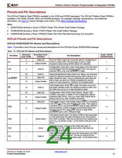
Table 13: XCFxxP Pin Names and Descriptions (VO48/VOG48 and FS48/FSG48)
48-pin
48-pin
TFBGA
(FS48/
FSG48)
Boundary-
Boundary-
Scan Order
TSOP
(VO48/
VOG48)
Pin Name
Scan
Pin Description
Function
28
27
26
25
24
23
22
21
20
19
18
17
16
15
14
13
Data Out
Output Enable
Data Out
D0
D1
D2
D3
D4
D5
D6
D7
28
29
32
33
43
44
47
48
H6
H5
E5
D5
C5
B5
A5
A6
Output Enable
Data Out
D0 is the DATA output pin to provide data for configuring an
FPGA in serial mode.
D0-D7 are the DATA output pins to provide parallel data for
configuring a Xilinx FPGA in SelectMap (parallel) mode.
The D0 output is set to a high-impedance state during ISPEN
(when not clamped).
The D1-D7 outputs are set to a high-impedance state during
ISPEN (when not clamped) and when serial mode is selected
for configuration. The D1-D7 pins can be left unconnected
when the PROM is used in serial mode.
Output Enable
Data Out
Output Enable
Data Out
Output Enable
Data Out
Output Enable
Data Out
Output Enable
Data Out
Output Enable
Configuration Clock Input. An internal programmable control bit
selects between the internal oscillator and the CLK input pin as
the clock source to control the configuration sequence. Each
rising edge on the CLK input increments the internal address
counter if the CLK input is selected, CE is Low, OE/RESET is
High, BUSY is Low (parallel mode only), and CF is High.
CLK
01
Data In
12
B3
04
03
Data In
Output Enable/Reset (Open-Drain I/O).
When Low, this input holds the address counter reset and the
DATA and CLKOUT outputs are placed in a high-impedance
state. This is a bidirectional open-drain pin that is held Low
Data Out
OE/RESET
11
13
A3
B4
02
00
Output Enable while the PROM completes the internal power-on reset
sequence. Polarity is not programmable.
Data In
Chip Enable Input. When CE is High, the device is put into
low-power standby mode, the address counter is reset, and
the DATA and CLKOUT outputs are placed in a high-
impedance state.
CE
Configuration Pulse (Open-Drain I/O). As an output, this pin
allows the JTAG CONFIG instruction to initiate FPGA
11
10
Data In
configuration without powering down the FPGA. This is an
open-drain signal that is pulsed Low by the JTAG CONFIG
command. As an input, on the rising edge of CF, the current
design revision selection is sampled and the internal address
counter is reset to the start address for the selected revision.
If unused, the CF pin must be pulled High using an external
Data Out
CF
6
D1
09
Output Enable
4.7 kΩ pull-up to VCCO
.
DS123 (v2.18) May 19, 2010
www.xilinx.com
Product Specification
26

 XILINX [ XILINX, INC ]