R
Platform Flash In-System Programmable Configuration PROMs
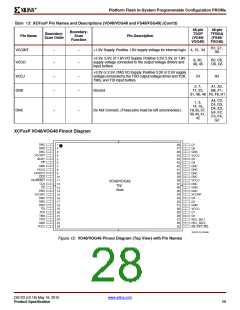
Table 13: XCFxxP Pin Names and Descriptions (VO48/VOG48 and FS48/FSG48) (Cont’d)
48-pin
TSOP
(VO48/
VOG48)
48-pin
TFBGA
(FS48/
FSG48)
Boundary-
Boundary-
Pin Name
Scan
Pin Description
Scan Order
Function
B1, E1,
G6
VCCINT
–
–
–
–
+1.8V Supply. Positive 1.8V supply voltage for internal logic. 4, 15, 34
+3.3V, 2.5V, or 1.8V I/O Supply. Positive 3.3V, 2.5V, or 1.8V
supply voltage connected to the output voltage drivers and
input buffers.
8, 30,
38, 45
B2, C6,
D6, G5
VCCO
VCCJ
GND
+3.3V or 2.5V JTAG I/O Supply. Positive 3.3V or 2.5V supply
voltage connected to the TDO output voltage driver and TCK,
TMS, and TDI input buffers.
–
–
–
–
24
H2
2, 7,
17, 23,
A1, A2,
B6, F1,
Ground
31, 36, 46 F5, F6, H1
A4, C3,
1, 3,
C4, D3,
14, 16,
D4, E3,
18,35,37,
E4, F2,
39,40,41,
F3, F4,
DNC
–
–
Do Not Connect. (These pins must be left unconnected.)
42
G2
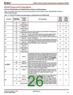
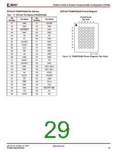
XCFxxP VO48/VOG48 Pinout Diagram
X-Ref Target - Figure 12
DNC
GND
DNC
48
47
46
45
44
43
42
41
40
39
D7
D6
GND
VCCO
D5
D4
DNC
DNC
DNC
DNC
VCCO
DNC
GND
DNC
VCCINT
D3
D2
GND
VCCO
D1
1
2
3
4
5
6
7
8
VCCINT
BUSY
CF
GND
VCCO
CLKOUT
CEO
OE/RESET
CLK
CE
DNC
VCCINT
DNC
9
10
11
12
13
14
15
16
17
18
19
20
21
22
23
24
38
37
36
35
VO48/VOG48
Top
View
34
33
32
31
30
29
28
27
26
25
GND
DNC
TDI
TCK
TMS
TDO
GND
VCCJ
D0
REV_SEL1
REV_SEL0
EN_EXT_SEL
DS123_24_031908
Figure 12: VO48/VOG48 Pinout Diagram (Top View) with Pin Names
DS123 (v2.18) May 19, 2010
www.xilinx.com
Product Specification
28

 XILINX [ XILINX, INC ]