X4043/45
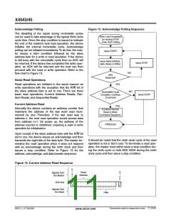
The state of the control register can be read at any
time by performing a random read at address 1FFh,
using the special preamble. Only one byte is read by
each register read operation. The X4043/45 resets
itself after the first byte is read. The master should sup-
ply a stop condition to be consistent with the bus proto-
col, but a stop is not required to end this operation.
WD1, WD0: Watchdog Timer Bits
The bits WD1 and WD0 control the period of the watch-
dog timer.The options are shown below.
WD1
WD0
Watchdog Time Out Period
1.4 seconds
0
0
1
1
0
1
0
1
600 milliseconds
7
6
5
4
3
2
1
0
200 milliseconds
0
WD1 WD0 BP1 BP0 RWEL WEL BP2
Disabled (factory setting)
RWEL: Register Write Enable Latch (Volatile)
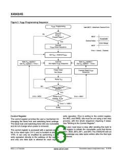
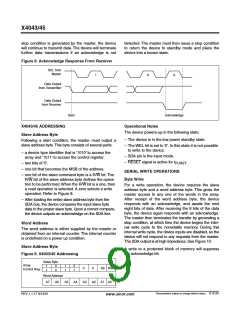
Writing to the Control Register
The RWEL bit must be set to “1” prior to a write to the
Control Register.
Changing any of the nonvolatile bits of the control reg-
ister requires the following steps:
– Write a 02H to the control register to set the write
enable latch (WEL). This is a volatile operation, so
there is no delay after the write. (Operation pre-
ceeded by a start and ended with a stop).
WEL: Write Enable Latch (Volatile)
The WEL bit controls the access to the memory and to
the Register during a write operation. This bit is a vola-
tile latch that powers up in the LOW (disabled) state.
While the WEL bit is LOW, writes to any address,
including any control registers will be ignored (no
acknowledge will be issued after the Data Byte). The
WEL bit is set by writing a “1” to the WEL bit and
zeroes to the other bits of the control register. Once
set, WEL remains set until either it is reset to 0 (by writ-
ing a “0” to the WEL bit and zeroes to the other bits of
the control register) or until the part powers up again.
Writes to the WEL bit do not cause a nonvolatile write
cycle, so the device is ready for the next operation
immediately after the stop condition.
– Write a 06H to the control register to set both the
register write enable latch (RWEL) and the WEL bit.
This is also a volatile cycle. The zeros in the data
byte are required. (Operation preceeded by a start
and ended with a stop).
– Write a value to the control register that has all the
control bits set to the desired state. This can be rep-
resented as 0xys t01r in binary, where xy are the WD
bits, and rst are the BP bits. (Operation preceeded
by a start and ended with a stop). Since this is a non-
volatile write cycle it will take up to 10ms to com-
plete. The RWEL bit is reset by this cycle and the
sequence must be repeated to change the nonvola-
tile bits again. If bit 2 is set to ‘1’ in this third step
(0xys t11r) then the RWEL bit is set, but the WD1,
WD0, BP2, BP1 and BP0 bits remain unchanged.
Writing a second byte to the control register is not
allowed. Doing so aborts the write operation and
returns a NACK.
BP2, BP1, BP0: Block Protect Bits (Nonvolatile)
The block protect bits, BP2, BP1 and BP0, determine
which blocks of the array are write protected. A write to
a protected block of memory is ignored. The block pro-
tect bits will prevent write operations to one of eight
segments of the array.
Protected Addresses
– A read operation occurring between any of the previ-
ous operations will not interrupt the register write
operation.
(Size)
Array Lock
None
0
0
0
0
1
1
1
1
0
0
1
1
0
0
1
1
0
1
0
1
0
1
0
1
None (factory setting)
180h - 1FFh (128 bytes)
Upper 1/4 (Q4)
– The RWEL bit cannot be reset without writing to the
nonvolatile control bits in the control register, power
cycling the device or attempting a write to a write
protected block.
100h - 1FFh (256 bytes) Upper 1/2 (Q3,Q4)
000h - 1FFh (512 bytes)
000h - 00Fh (16 bytes)
000h - 01Fh (32 bytes)
000h - 03Fh (64 bytes)
000h - 07Fh (128 bytes)
Full Array (All)
First Page (P1)
First 2 pgs (P2)
First 4 pgs (P4)
First 8 pgs (P8)
To illustrate, a sequence of writes to the device consist-
ing of [02H, 06H, 02H] will reset all of the nonvolatile
bits in the control register to 0. A sequence of [02H,
06H, 06H] will leave the nonvolatile bits unchanged
and the RWEL bit remains set.
Characteristics subject to change without notice. 7 of 25
REV 1.1.17 9/14/01
www.xicor.com

 XICOR [ XICOR INC. ]