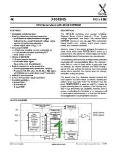
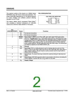
X4043/45
Setting a V
Voltage
CASE B
TRIP
There are two procedures used to set the threshold
voltages (V ), depending if the threshold voltage to
Now if the V
(desired), perform the reset sequence as described in
the next section. The new V voltage to be applied
(actual), is higher than the V
TRIP
TRIP
TRIP
be stored is higher or lower than the present value. For
example, if the present V is 2.9 V and the new
TRIP
(desired) – (V
TRIP
to V
will now be: V
(actual) –
CC
TRIP
TRIP
V
is 3.2 V, the new voltage can be stored directly
TRIP
V
(desired)).
TRIP
into the V
cell. If however, the new setting is to be
TRIP
Note: This operation does not corrupt the memory
array.
lower than the present setting, then it is necessary to
“reset” the V voltage before setting the new value.
TRIP
Setting a Lower V
Voltage
Setting a Higher V
Voltage
TRIP
TRIP
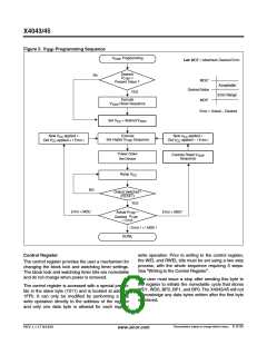
In order to set V
present value, then V
ing to the procedure described below. Once V
been “reset”, then V
to a lower voltage than the
must first be “reset” accord-
To set a V
threshold to a new voltage which is
TRIP
TRIP
higher than the present threshold, the user must apply
the desired V threshold voltage to the V .Then, a
programming voltage (Vp) must be applied to the WP
pin before a START condition is set up on SDA. Next,
issue on the SDA pin the Slave Address A0h, followed
TRIP
has
TRIP
TRIP
CC
can be set to the desired volt-
TRIP
age using the procedure described in “Setting a Higher
Voltage”.
V
TRIP
by the Byte Address 01h for V
and a 00h Data
TRIP
Resetting the V
Voltage
Byte in order to program V
. The STOP bit following
TRIP
TRIP
a valid write operation initiates the programming
sequence. WP pin must then be brought LOW to com-
plete the operation.
To reset a V
voltage, apply the programming volt-
TRIP
age (Vp) to the WP pin before a START condition is set
up on SDA. Next, issue on the SDA pin the Slave
Address A0h followed by the Byte Address 03h fol-
To check if the V
has been set, first power down
TRIP
lowed by 00h for the Data Byte in order to reset V
.
TRIP
the device. Slowly ramp up V
and observe when the
CC
The STOP bit following a valid write operation initiates
the programming sequence. Pin WP must then be
brought LOW to complete the operation.
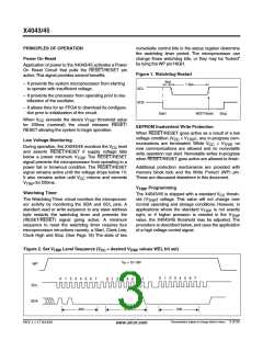
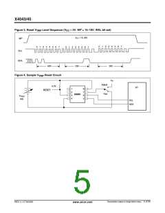
output, RESET (4043) or RESET (4045) switches. The
voltage at which this occurs is the V
Figure 2).
(actual) (see
TRIP
After being reset, the value of V
nal value of 1.7V or lesser.
becomes a nomi-
TRIP
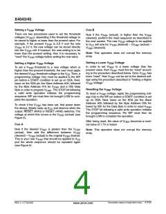
CASE A
Now if the desired V
is greater than the V
Note: This operation does not corrupt the memory
array.
TRIP
TRIP
TRIP
(actual), then add the difference between V
(desired) – V (actual) to the original V
desired.
TRIP
TRIP
This is your new V
that should be applied to V
TRIP
CC
and the whole sequence should be repeated again
(see Figure 5).
Characteristics subject to change without notice. 4 of 25
REV 1.1.17 9/14/01
www.xicor.com

 XICOR [ XICOR INC. ]