X4043/45
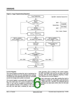
Figure 5. V
Programming Sequence
TRIP
V
Programming
Desired
TRIP
Let: MDE = Maximum Desired Error
No
V
<
TRIP
Present Value ?
MDE+
Acceptable
Desired Value
YES
Error Range
MDE–
Execute
Reset Sequence
V
TRIP
Error = Actual – Desired
Set V
= desired V
Execute
CC
TRIP
New V
applied =
New
applied =
CC
V
CC
Set Higher V
Sequence
V
Old V
applied – | Error |
Old
applied + | Error |
TRIP
CC
CC
Power Down
the Device
Execute Reset V
Sequence
TRIP
Ramp V
CC
NO
Output Switches?
(RESET)
YES
Error < MDE–
V
–
Error > MDE+
Actual
Desired
TRIP
V
TRIP
= Error
| Error | < | MDE |
DONE
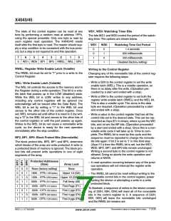
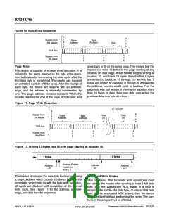
Control Register
write operation. Prior to writing to the control register,
the WEL and RWEL bits must be set using a two step
process, with the whole sequence requiring 3 steps.
See "Writing to the Control Register".
The control register provides the user a mechanism for
changing the block lock and watchdog timer settings.
The block lock and watchdog timer bits are nonvolatile
and do not change when power is removed.
The user must issue a stop after sending this byte to
the register to initiate the nonvolatile cycle that stores
WD1, WD0, BP2, BP1, and BP0.The X4043/45 will not
acknowledge any data bytes written after the first byte
is entered.
The control register is accessed with a special pream-
ble in the slave byte (1011) and is located at address
1FFh. It can only be modified by performing a byte
write operation directly to the address of the register
and only one data byte is allowed for each register
Characteristics subject to change without notice. 6 of 25
REV 1.1.17 9/14/01
www.xicor.com

 XICOR [ XICOR INC. ]