X4043/45
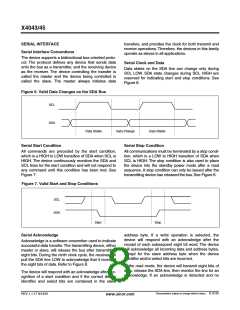
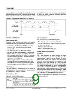
stop condition is generated by the master, the device
will continue to transmit data. The device will terminate
further data transmissions if an acknowledge is not
detected. The master must then issue a stop condition
to return the device to standby mode and place the
device into a known state.
Figure 8. Acknowledge Response From Receiver
SCL from
Master
1
8
9
Data Output
from Transmitter
Data Output
from Receiver
Start
Acknowledge
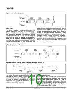
X4043/45 ADDRESSING
Slave Address Byte
Operational Notes
The device powers-up in the following state:
– The device is in the low power standby state.
Following a start condition, the master must output a
slave address byte.This byte consists of several parts:
– The WEL bit is set to ‘0’. In this state it is not possible
to write to the device.
– a device type identifier that is ‘1010’ to access the
array and ‘1011’ to access the control register.
– SDA pin is the input mode.
– RESET signal is active for t
.
PURST
– two bits of ‘0’.
– one bit that becomes the MSB of the address.
SERIAL WRITE OPERATIONS
Byte Write
– one bit of the slave command byte is a R/W bit. The
R/W bit of the slave address byte defines the opera-
tion to be performed.When the R/W bit is a one, then
a read operation is selected. A zero selects a write
operation. Refer to Figure 8.
For a write operation, the device requires the slave
address byte and a word address byte. This gives the
master access to any one of the words in the array.
After receipt of the word address byte, the device
responds with an acknowledge, and awaits the next
eight bits of data. After receiving the 8 bits of the data
byte, the device again responds with an acknowledge.
The master then terminates the transfer by generating a
stop condition, at which time the device begins the inter-
nal write cycle to the nonvolatile memory. During this
internal write cycle, the device inputs are disabled, so the
device will not respond to any requests from the master.
The SDA output is at high impedance. See Figure 10.
– After loading the entire slave address byte from the
SDA bus, the device compares the input slave byte
data to the proper slave byte. Upon a correct compare,
the device outputs an acknowledge on the SDA line.
Word Address
The word address is either supplied by the master or
obtained from an internal counter. The internal counter
is undefined on a power up condition.
Slave Address Byte
Figure 9. X4043/45 Addressing
Slave Byte
A write to a protected block of memory will suppress
the acknowledge bit.
Array
1
0
1
0
0
0
A8 R/W
Control Reg.
1
0
1
1
Word Address
A7 A6
A5
A4
A3
A2 A1 A0
Characteristics subject to change without notice. 9 of 25
REV 1.1.17 9/14/01
www.xicor.com

 XICOR [ XICOR INC. ]