X1241 – Preliminary Information
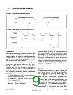
Figure 8. Valid Start and Stop Conditions
SCL
SDA
Start
Stop
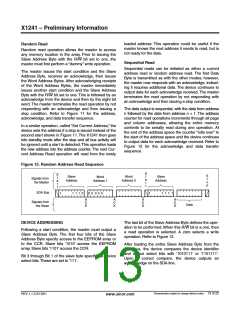
Figure 9. Acknowledge Response From Receiver
SCL from
Master
1
8
9
Data Output from
Transmitter
Data Output
from Receiver
Start
Acknowledge
Acknowledge
In the read mode, the device will transmit eight bits of
data, release the SDA line, then monitor the line for an
acknowledge. If an acknowledge is detected and no
stop condition is generated by the master, the device
will continue to transmit data. The device will terminate
further data transmissions if an acknowledge is not
detected. The master must then issue a stop condition
to return the device to Standby mode and place the
device into a known state.
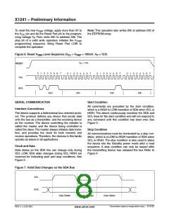
Acknowledge is a software convention used to indicate
successful data transfer. The transmitting device, either
master or slave, will release the bus after transmitting
eight bits. During the ninth clock cycle, the receiver will
pull the SDA line LOW to acknowledge that it received
the eight bits of data. Refer to Figure 5.
The device will respond with an acknowledge after rec-
ognition of a start condition and if the correct Device
Identifier and Select bits are contained in the Slave
Address Byte. If a write operation is selected, the
device will respond with an acknowledge after the
receipt of each subsequent eight bit word. The device
will acknowledge all incoming data and address bytes,
except for:
WRITE OPERATIONS
Byte Write
For a byte write operation, the device requires the
Slave Address Byte and the Word Address Bytes. This
gives the master access to any one of the words in the
array or CCR. (Note: Prior to writing to the CCR, the
master must write a 02h, then 06h to the status regis-
ter in preceding operations to enable the write opera-
tion. See “Writing to the Clock/Control Registers” on
page 6.) Upon receipt of each address byte, the X1241
responds with an acknowledge. After receiving both
address bytes the X1241 awaits the eight bits of data.
After receiving the 8 data bits, the X1241 again
responds with an acknowledge. The master then
– The Slave Address Byte when the Device Identifier
and/or Select bits are incorrect
– All Data Bytes of a write when the WEL in the Write
Protect Register is LOW
– The 2nd Data Byte of a Register Write Operation
(when only 1 data byte is allowed)
Characteristics subject to change without notice. 9 of 22
REV 1.1.3 2/13/01
www.xicor.com

 XICOR [ XICOR INC. ]